Continue to Site

Welcome to EDAboard.com

Welcome to our site! EDAboard.com is an international Electronics Discussion Forum focused on EDA software, circuits, schematics, books, theory, papers, asic, pld, 8051, DSP, Network, RF, Analog Design, PCB, Service Manuals... and a whole lot more! To participate you need to register. Registration is free. Click here to register now.

PIC controlling AC loads

Status
Not open for further replies.
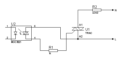
Hehe.. I don't see them the same... A2 is MT1 while A1 is MT2
The input junction of the upper one is G-A2 ... while of the lower is G-MT1

By the way can we give names to the 3 terminals... Gate is one... what about the other two :)
 

Hehe.. I don't see them the same... A2 is MT1 while A1 is MT2
The input junction of the upper one is G-A2 ... while of the lower is G-MT1

In both circuits, A2/MT2 is connected to Live. MT1/A1 is connected via load to Neutral. MT2/A2 goes to opto-triac. From the other pin from the opto-triac, a resistor goes to Gate. [In both circuits].

---------- Post added at 22:34 ---------- Previous post was at 22:32 ----------

Why not just refer to them as A1 and A2? :grin:
 

It seems... to you it doesn't matter how the gate is drawn it can be close to any of the two terminals without making any difference!

Sorry may I ask you if you did try to measure by an ohmmeter (which is able to test a diode) the impedance between each pair of the triac terminals?
 

The gate is obviously referenced. Please take a look at the circuits carefully. I've placed them side-by-side in post 40. A2 IS MT2 and A1 IS MT1.

---------- Post added at 22:39 ---------- Previous post was at 22:37 ----------

Ok, let's use BTA26. From the datasheet, we see pin 1 is A1/MT1 and pin 2 is A2/MT2. So, think of it like that.

---------- Post added at 22:40 ---------- Previous post was at 22:39 ----------

Sorry may I ask you if you did try to measure by an ohmmeter (which is able to test a diode) the impedance between each pair of the triac terminals?

Nope. I haven't tried it.
 

hi tahmid..

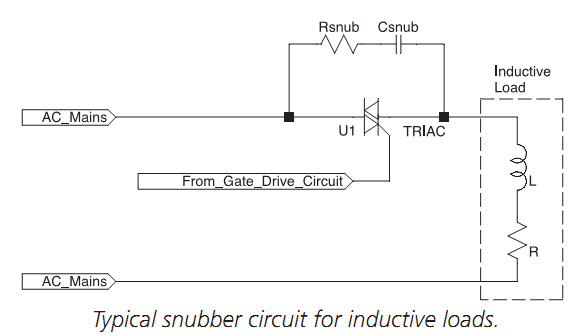
where do the snubber will be placed? in the input of the optoisolator right?
I have always seen a diode place in some relays but I just knew now that it is called snubber.. hehe thanks
58_1311177476.png
 

No... A1 is far from the gate on the drawing ... while MT1 is close to the gate.

So A1 is MT2 and A2 id MT1 on the pics
 

Just to clarify, the software I used for drawing does not have A1 or A2 written. I just wrote them on the triac to clarify the direction.

On my side, I reply one what I see ... I don't care if the labels are K1/K2... MT4/M6 :) I just look where the gate is drawn. the terminal far from it can provide the trigger current.

In other words, when using an opto... the loop is:
The triac terminal far from the gate... a resistor... opto triac... gate...
 

Reason why we need a snubber:

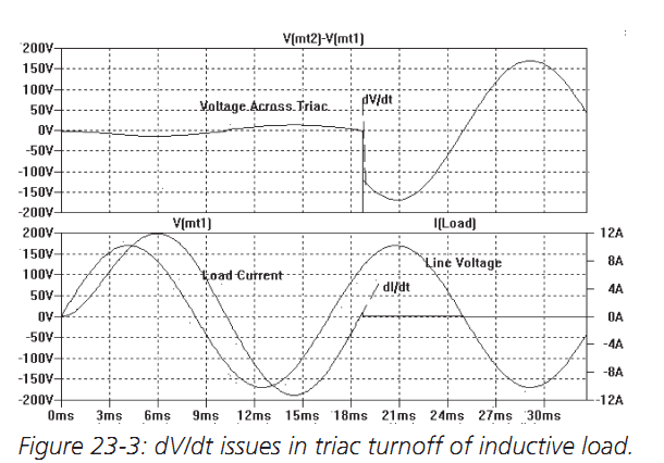
But, suppose we have an inductive load, such as motor. The current and voltage through the triac and the load are no longer in phase, as illustrated in Figure23-3. At the time the triacsnaps into non-conductive mode, the voltage across the triac is, in the worst case (for a phase angle of 90° between V and I) the peak line voltage. And, the triac’s switching speed maybe on the order of a few microseconds or less. Hence, dV/dt can easily reach hundreds of volts/microsecond. The actual dV/dt depends on the load, stray inductance and capacitance and the triac’s parameters.
A common solution todV/dt problems is to add an RC-snubber network across the triac, as shown. The RC network slows the rate of change in applied voltage and thus drops the dV/dt below the triac’s rating.

33_1311180390.png


Hope this helps.
Tahmid.
 

On my side, I reply one what I see ... I don't care if the labels are K1/K2... MT4/M6 :) I just look where the gate is drawn. the terminal far from it can provide the trigger current.

In other words, when using an opto... the loop is:
The triac terminal far from the gate... a resistor... opto triac... gate...

I see your confusion. In the datasheet you can see that A1 is the point near the gate. In the circuit, it's drawn differently, so I added the labels A1 and A2 to make it clear.

---------- Post added at 22:56 ---------- Previous post was at 22:52 ----------

In my inverter, I used 100 ohm 2W resistor and 0.1uF 630V capacitor. In the book I was referring to, the author mentions the use of a 39 ohm resistor and 0.01uF capacitor.
 

You are right. When the triac turns on, the inductive load keeps passing a current through it (lagging current). But when this current becomes zero, the voltage on the triac rises rather quickly to follow the wave of mains voltage. This fast change induces an internal current to the gate (via internal capacitance) which turns on the triac without an external trigger. The snubber damps this high dV/dt

---------- Post added at 20:05 ---------- Previous post was at 19:59 ----------

It should be across the triac:
70_1311180275.png

Post #49, the node above the word TRIAC should be connected to the drive circuit (assuming no isolation) so that a current can flow between the gate and this node.
I always let the direction of the gate current to be out of the gate. The trigger current is lower (higher sensitivity) in this direction than if it is done in reverse.
 
Last edited:

Yes. Now I get your point. You were talking about the drive circuit referring to the symbol, I was talking referring to MT1/MT2. To clear the confusion, MT1/A1 is the point closer to the gate, in the above circuit, it is the node above the word TRIAC. MT2/A2 is the point farther away from the gate.
 

I see now your point... but to me I can't avoid contemplating the symbol :) while you were admiring the labels :grin:

I knew there is something missing... because I was sure that you too have a good experience in this.
 

Status
Not open for further replies.

Similar threads

Part and Inventory Search

Welcome to EDABoard.com

Sponsor

Back
Top