Continue to Site

Welcome to EDAboard.com

Welcome to our site! EDAboard.com is an international Electronics Discussion Forum focused on EDA software, circuits, schematics, books, theory, papers, asic, pld, 8051, DSP, Network, RF, Analog Design, PCB, Service Manuals... and a whole lot more! To participate you need to register. Registration is free. Click here to register now.

[SOLVED] Pic 16f876a Pure Sinewave inverter

Status
Not open for further replies.
what about software changes for feedback values? Is there any need to modify it?
 
  • Like
Reactions: tearq

    tearq

    Points: 2
    Helpful Answer Positive Rating
Hello, I'm looking for some pure sinewave inverter. Cause I'm now writing and almost finishing my diploma thesis where is practical major small photovoltaic power plant. Now I have this schematic:

PV panel, DC/DC converter with PIC16F876A, battery and trivial dc/ac inverter with square wave.

So I need to find some pure sinewave inv with switcher "220V,Charge/Ups" which is in modified schematic by maharadga, could u help me please?

I will analyze back influence of my power plant and I need pure sinewave inverter.

Thanx so much.
 
  • Like
Reactions: tearq

    tearq

    Points: 2
    Helpful Answer Positive Rating
Hello to all.
My inverter work fine. If increase the power, inverter stop, and both led no light. After a few second inverter go to start. It is OK.
I have no idea where to change to increase the maximal power with 10%?
I think may put a resistor in parallel with the current transformer (secondary), but I do not know the value.

Best regards
 
  • Like
Reactions: tearq

    tearq

    Points: 2
    Helpful Answer Positive Rating
Very nice!
Maybe you should use a trimer pot. with value of ~ 47kohm or higher and then carefully experiment with correct position, but you have to check ACU voltage also.

Regards
 
Re: pwm inverter circuits

My design is a sine-wave stand-alone PWM voltage-source inverter (Not UPS)
with PIC16F876A MCU, with parameters: Uin=12V DC, Uo=230V AC, 50Hz, P=500W.
Inverter have an integrated input under/over voltage protection, output voltage regulation, output current protection and overtemperature protection.
Output voltage is a pure sine-wave, generated with built-in PWM module of PIC MCU,
with frequency 20Khz.
:D

Hi Taner

I have a doubt in the sircuit

is this inverter has any standby source like AC power?

What about re charging the battery

Regards

Suresh
 
  • Like
Reactions: tearq

    tearq

    Points: 2
    Helpful Answer Positive Rating
Re: pwm inverter circuits

hi Mr.Taner and all of friends
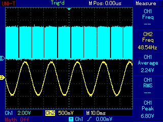
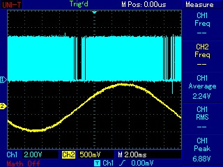
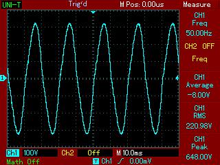
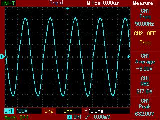
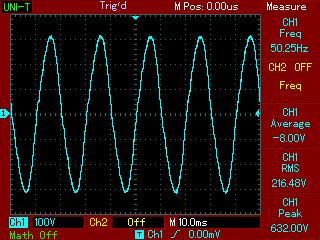
I would like to discuss some issues in his inverter design. This design is so interest. I also tested and constructed it. The output is fine results. But, at the output voltage's amplitude is around 170Vac, Pure sine wave form is stable. In order to get the 200 Vac we adjust the gain of the voltage sensing amplifier. However, it can not handle to the variable load. It is stable at 20 Watts (small load). We would like to handle more load to the desired 550 Watts and more. So Some of the factors and source code Program will be updated. I would like to post of my testing results as well as simulations and experimental test results as attachments in order to discuss and suggest for the improvement of taner's design. I would like to thanks a lot for all friends in our forum.
all of friends, After downloaded and seen my experimental results, Pls give me valuable suggestions and advices.
with regards
thuhtay

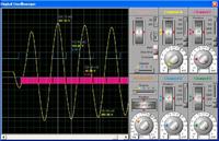
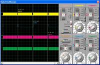
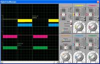
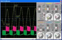
Simulation results
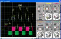
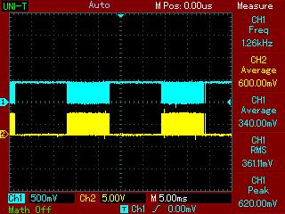
88_1306272200.jpgSimulation Output Waveform of Pure Sine Wave Inverter
24_1306272200.jpgPeriodic PWM signals and Directional signal
52_1306272200.jpgPWM output signals of the Pre-driver circuitries
42_1306272200.jpgPWM Output Waveforms of the High Side MOSFETs57_1306272200.jpgPWM Output Waveform of the Low Sided MOSFETs

Experimental Test results
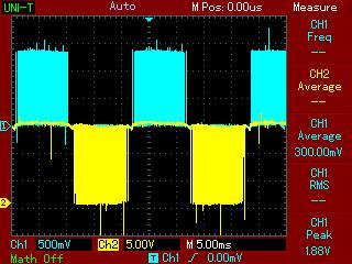
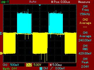
33_1306273052.jpg
39_1306273052.jpg
1_1306273052.jpg
86_1306273052.jpg
26_1306273052.jpg

19_1306273120.jpg


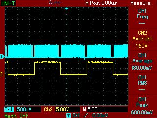
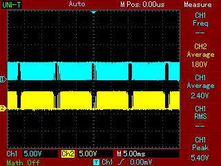
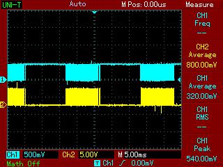
Here, we can see that simulation and experimental results are same as the desired outputs
 
Last edited:
  • Like
Reactions: tearq

    tearq

    Points: 2
    Helpful Answer Positive Rating
Hi all friends
Here, we can see the results of pure sine wave output with respect to 20 kHz PWM signals. It output waveform is so clean sine wave but the voltage amplitude is about maximum 170 Vac nearly. So, how do you exchange or update the program source code or circuitries. I will be discuss the notable point in source code with all friends in coming next post.

30_1306315123.jpg
70_1306315123.jpg

with regrads
thuhtay
 
  • Like
Reactions: tearq

    tearq

    Points: 2
    Helpful Answer Positive Rating
Hello Friendz,

This is my first touch in inverter circuits experience, & I have decided to design and build a true sine wave inverter as my final year project. It seems interested here because im sure my fellow technical friends will help me out, so pls do help me for my up coming doubts regarding my project.

Regards
 

thuhtay some of our friends had the same problem before, you need to go through the whole thread, so you can know which type of problems arised in this circuits and how they removed, once you go through, you can get answers to many of your questions, its recommended, we all are here to help, but there is always a home work before a constructive discussion

Best Regards
 

Hi jami007 and all of friends, Californiajoe
My problem is accomplished, the output voltage is about 230 Vac, the expected average efficiency is about 70%. Do you experiment this inverter design with load test. In my load test experiment, it can be handle good efficiency and pure sine waveform at 300 Watts. And then, In 400 watts and 500 watts load conditions, the output voltage slightly decreased and the waveform is clipped at the peaks. To handle more output power, I think that we will be upgrade taner's design with switch mode type.
maharadga is also continue to construct UPS design. I also interest his work. But, I think that he consider the current sensing output is adjust at fixed 2.5 V signals and also Other circuitries such as a/b sensing is changed. I think it will be change either source code or use without ab sensing source code. I also want to discuss maharadga for his research.
The next experimental results are also posted. Thank for interesting our blog!!!


47_1306576906.jpg
67_1306576906.jpg
59_1306576906.jpg
60_1306576906.jpg
49_1306576906.jpg

I would like to meet Mr.Taner again in this post to discuss logical consideration of his source code. Moreover, To improve this design and upgrade other facilities, we should be discuss with all friends especially the pioneer designer Mr.Taner
with respects
thuhtay
 

hi tanner
this is my first time in this forum.
could you please tell us how to write the program in assembly code, only the lookup table and the output voltage regulation
thanks

---------- Post added at 03:09 ---------- Previous post was at 02:47 ----------

hi tanner
this is my first time in this forum.
could you please tell us how to write the program in assembly code, only the lookup table and the output voltage regulation
thanks

---------- Post added at 03:11 ---------- Previous post was at 03:09 ----------

hi tanner
this is my first time in this forum.
could you please tell us how to write the program in assembly code, only the lookup table and the output voltage regulation
thanks
 

Very good work. New disighn for PCB looks excelent. If I see correct, your transformar has double coil?
With increasing of the load you have to check also Ubat.

Regards
 
  • Like
Reactions: tearq

    tearq

    Points: 2
    Helpful Answer Positive Rating
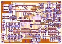
Some time ago Taner told that this inverter works fine under 300 watts load, thuhtay can you please send me the PCB layout of the circuit, also will you please post the models of current and Voltage Transformers

Best Regards
 

Hi jami007
I think that A'/B signal is not 50Hz PWM signal in the C program source. It is only the directional signals 1 or 0 in order to alternate switching 20kHz PWM for 50 Hz half-cycle sine wave using SN74HC257D multiplexer. It is the command to generate the each driven PWM for positive half cycle and negative half cycle. I think the CCP2 PWM module is not used in this algorithm. It can see that the switching 20kHz PWM signals within 50Hz are generating sequentially using CCP1 PWM module with respect to the sine look up table 32- bits PWM duty cycle array. how do you think it is true?

---------- Post added at 22:18 ---------- Previous post was at 22:09 ----------

Californiajoe please mention hex file is for which device??? 16F876A or 16F877A???

---------- Post added at 04:05 PM ---------- Previous post was at 03:54 PM ----------

SN74HC257 is a data line selector

when A'/B= L it will give value from A at output (L or H), B is dont care
when A'/B= H it will give value from B at output (L or H), A is dont care
( G'= L to enable chip)

I think it should be more like PWM

---------- Post added at 04:09 PM ---------- Previous post was at 04:05 PM ----------

LM393 is a dual comparator, output should be PWM and PWM' at pin 1 and 7, check this on scope

---------- Post added at 04:11 PM ---------- Previous post was at 04:09 PM ----------

A'/B is a 50Hz sine wave signal

---------- Post added at 04:14 PM ---------- Previous post was at 04:11 PM ----------

ohh.... sorry.... A'/B is a square wave 50Hz, 50% duty cycle signal

Hi jami007
I think that A'/B signal is not 50Hz PWM signal in the C program source. It is only the directional signals 1 or 0 in order to alternate switching 20kHz PWM for 50 Hz half-cycle sine wave using SN74HC257D multiplexer. It is the command to generate the each driven PWM for positive half cycle and negative half cycle. I think the CCP2 PWM module is not used in this algorithm. It can see that the switching 20kHz PWM signals within 50Hz are generating sequentially using CCP1 PWM module with respect to the sine look up table 32- bits PWM duty cycle array. how do you think it is true?

---------- Post added at 23:13 ---------- Previous post was at 22:18 ----------

Some time ago Taner told that this inverter works fine under 300 watts load, thuhtay can you please send me the PCB layout of the circuit, also will you please post the models of current and Voltage Transformers

Best Regards
Hi fri 'jami007'
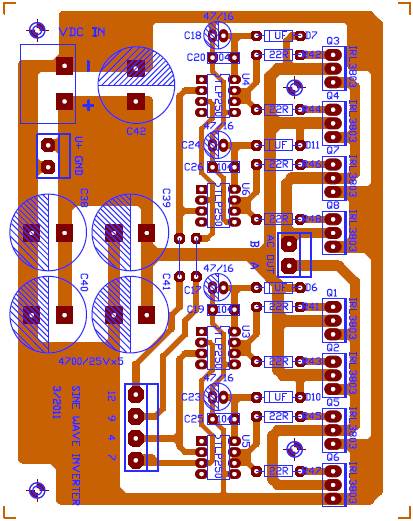
I posted my PCB design which is developed by using Circuit Maker 2000. Current transformer is constructed with reference (https://www.es.co.th/Schemetic/PDF/TZ2L9-TAEH.PDF). The Output Transformer rating is around 8Vac (Primary) to 250 Vac (secondary) E-I iron core low frequency transformer (50Hz).

Switching Controller PCB Design

H-Bridge Inverter PCB Design
7_1306879730.jpg

Best regards
 
Last edited:
I just gave the example of pwm in this algorithm, A'/B is a square wave 50Hz, 50% duty cycle signal

---------- Post added at 10:49 ---------- Previous post was at 10:48 ----------

you are so right it is only directional signal 1 or 0
 

Hi jami007
I think that A'/B signal is not 50Hz PWM signal in the C program source. It is only the directional signals 1 or 0 in order to alternate switching 20kHz PWM for 50 Hz half-cycle sine wave using SN74HC257D multiplexer. It is the command to generate the each driven PWM for positive half cycle and negative half cycle. I think the CCP2 PWM module is not used in this algorithm. It can see that the switching 20kHz PWM signals within 50Hz are generating sequentially using CCP1 PWM module with respect to the sine look up table 32- bits PWM duty cycle array. how do you think it is true?

---------- Post added at 22:18 ---------- Previous post was at 22:09 ----------


Hi jami007
I think that A'/B signal is not 50Hz PWM signal in the C program source. It is only the directional signals 1 or 0 in order to alternate switching 20kHz PWM for 50 Hz half-cycle sine wave using SN74HC257D multiplexer. It is the command to generate the each driven PWM for positive half cycle and negative half cycle. I think the CCP2 PWM module is not used in this algorithm. It can see that the switching 20kHz PWM signals within 50Hz are generating sequentially using CCP1 PWM module with respect to the sine look up table 32- bits PWM duty cycle array. how do you think it is true?

---------- Post added at 23:13 ---------- Previous post was at 22:18 ----------


Hi fri 'jami007'
I posted my PCB design which is developed by using Circuit Maker 2000. Current transformer is constructed with reference (https://www.es.co.th/Schemetic/PDF/TZ2L9-TAEH.PDF). The Output Transformer rating is around 8Vac (Primary) to 250 Vac (secondary) E-I iron core low frequency transformer (50Hz).

Switching Controller PCB Design

H-Bridge Inverter PCB Design
7_1306879730.jpg

Best regards


Nice design can you please share circuit maker 2000 design file

thanking you

Fragrance
 

Hi maharadga
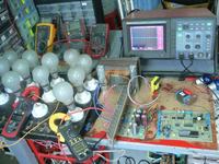
I think you are going to construct the UPS version of the Sine Wave inverter. Maharadga, I would like to discuss about My experimental load test. According to taner's design, Pic16F876/877A pure sine wave inverter had been constructed. After that, I tested this inverter with variable loads. Firstly, I used 100 Watts light bulbs as the resistive loads. In this experiment, it can be defined that its' optimal Output power rating is nearly about 300 Watts. As it can be seen in my experimental results in Page 34. I also tested it with inductive loads with cooler fan. It is also Ok with stable sine wave. However, It is not reliable with capacitive loads test experiment such as my personal computer. I notice that taners' design is not reliable with capacitive load. It is not handle in capacitive nature in my experiments. Do you notice that? If you will test this condition, could you share your valuable advice and suggestions to me. I always look forward to discuss with you and Mr. Taner.
with regrads
thuhtay

---------- Post added at 22:28 ---------- Previous post was at 21:55 ----------

Hi californiajoe, jami007,
The above post is my experience from testing my experiment with capacitive loads such as my personal desktop computer. So we are going to the UPS version to reliable with computer, I think this fact is should be noticed that the output voltage fluctuation and wave shape deformed in capacitive load test experiment. If you notice that this point, How do you solve this problem? I will expect your valuable advice and suggestions.
with regrads
thuhtay
 

Nice design can you please share circuit maker 2000 design file

thanking you

Fragrance

hi Fragrance
I posted the PCB design for the Pure Sine Wave Inverter. Good Luck for your experiment. Sorry for my delay to post this file.
with regards
thuhtay
 

Attachments

  • SINE WAVE INV.B.rar
    18.4 KB · Views: 967
hello to all
what about the charging of battery. I think boost converter used as battery charging in the ups version
 
Last edited:

Status
Not open for further replies.

Part and Inventory Search

Welcome to EDABoard.com

Sponsor

Back
Top