Continue to Site

Welcome to EDAboard.com

Welcome to our site! EDAboard.com is an international Electronics Discussion Forum focused on EDA software, circuits, schematics, books, theory, papers, asic, pld, 8051, DSP, Network, RF, Analog Design, PCB, Service Manuals... and a whole lot more! To participate you need to register. Registration is free. Click here to register now.

[SOLVED] Pic 16f876a Pure Sinewave inverter

Status
Not open for further replies.
these behave like select line for a multiplexer.....read MC14053BF datasheet and look for the table and try to understand...in our case A and C is combined so our intrested cases are A & C having same value and all other possible cases for B....
e.g A=C=0, B=0 etc... i hope u can understand logical operations.....

Added after 10 minutes:

Vlado can u plz note down your experimental results and testing circuits so when i start work again it will be helpful for me and aslo for others....and one thing more can you plz tell me how u test PIC on breadboard......i think u gave the desired values for normal operation externally from supply..????
 
MUX_A loks on osciloscop more like PWM, I am not sure about frequency becouse I didn't measure it and MUX_B looks like 50Hz square waves.

You must know that this signals are taken from MCU without any other chip. All inputs are connected to expected values of voltage. For example 2,5V you can get with two resistors, one is connected to gnd and another one to 5V. In the middle you have 2,5V. For other values you have to calculate resistors.
Like I said, next step is connectig 4053 with six new voltages (Curr_h, Curr_l, b, a, Volt and Stdby) and once again I'll check all outputs to get green light on LED.

Expected values for inputs you can not change (except in software), so hardware must give us proper values on there's outputs.

And finaly, every step will documented here.


Regards

Vlado

Added after 37 minutes:

I forgot before.
For example 2,5V you can get with two resistors (10k for example), one is connected to gnd and another one to 5V. In the middle you have 2,5V.

Vlado
 
in MUX case only important thing is the select line value..... e.g A=0 & B=0 which selects particular line and show it at output....i hope you know the working of a multiplexer and select lines.....so it will be more like pwm......giving 1 or 0 for a particular case......note down the value of A & B so u can determine output easily.......in our case we have 6 inputs and 3 outputs X,Y,Z of 4053....

Added after 8 minutes:

here are the top and bottom assembly pics.....
 
MC14053 is connected. Volt and Stdby signals are separated.
Decreiseing of Stdby stops PWM at 0,1V. Increaseing back Stdby, PWM is started at 1,9V and at 3,5V red and green LED start flashing for ten times after that only green LED is flashing and also PWM and AB flash with the same frequency.
Changing Volt signal from 0-5V has no efect on PWM at this point??

One question: I am using code from page two. Is this code correct, or no?

Regards
 
also read instructions for first time run provided in the working mannual

Added after 5 minutes:

volt signal is for output control from 170 to 230V, it was not working in my case too, maybe sensitivity is less, try larger resistance

Added after 6 minutes:

also check values at pin a and b with scope, these two are very important for inverter working
 

Reviewing the above PCB photos, I wonder what's the intended inverter power. I see supply traces with
about 2 mm width, good for maximum 6 - 8 A with standard 35 µm PCB, but I read about 500 VA on the schematic?

As another point, I noticed that the schematic diagramm (PIC16_Sine-wave_Inverter.pdf) shows a
wrong supply connection of low-side TLP250, but the PCB wiring seems to be different (hopefully correct).
 

Hi Friends,
Output supply traces is ~3.5mm width, for 230Vac this width is sufficient for 500VA output power. But for this power is required 24Vdc input power supply.
Project is still opened, not finished yet. I shared all altium project files and C code, and each of you can make required changes, useful for him.

Best regards,
Taner
 
Taner said:
Hi Friends,
Output supply traces is ~3.5mm width, for 230Vac this width is sufficient for 500VA output power. But for this power is required 24Vdc input power supply.
Project is still opened, not finished yet. I shared all altium project files and C code, and each of you can make required changes, useful for him.

Best regards,
Taner

Taner,

I appreciate your hardwork in bringing the beautiful circuit. For all of us can you plz post details of circuit, c program, schematic diagram finally once for all the members.

Once again thanks for the hard work.

With regards,
Elara
 
FvM said:
Reviewing the above PCB photos, I wonder what's the intended inverter power. I see supply traces with
about 2 mm width, good for maximum 6 - 8 A with standard 35 µm PCB, but I read about 500 VA on the schematic?

As another point, I noticed that the schematic diagramm (PIC16_Sine-wave_Inverter.pdf) shows a
wrong supply connection of low-side TLP250, but the PCB wiring seems to be different (hopefully correct).

can u plz tell which connection of tlp250 is wrong???? and there is no difference in schematics and PCB connection, I made it very carefully, may be there is a mistake in PCB followed by schematic.......There is no issue of PCB tracks on high quality double sided fiber sheet.....tracks widths are sufficient for this inverter and are attested by professionals......original size of board is about 7.6x8.1 inches....also u can reduce the size using smd components,but for ordinary components it is an average size, still its not the final vesion.......

Added after 1 minutes:

Mr Taner plz upload the final version of files related to the project

God Bless you
 

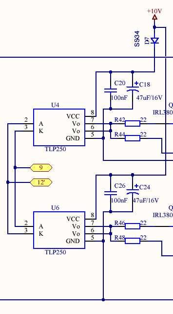
I'm talking of the detail shown below, VCC connection of U6. It's correct in Taner's schematic.

8_1282481278.jpg


Regarding PCB trace widths, Taner has said everything necessary. His PCB also shows, how a better primary
wiring for the high current nets can be done. Even if you provide 24V supply for a 500 VA inverter, which is
much better of course, it will still need about 22-25 A input current. Impossible with a 2 mm trace.
 
  • Like
Reactions: MN_TRI

    MN_TRI

    Points: 2
    Helpful Answer Positive Rating
FvM said:
I'm talking of the detail shown below, VCC connection of U6. It's correct in Taner's schematic.

8_1282481278.jpg


Regarding PCB trace widths, Taner has said everything necessary. His PCB also shows, how a better primary
wiring for the high current nets can be done. Even if you provide 24V supply for a 500 VA inverter, which is
much better of course, it will still need about 22-25 A input current. Impossible with a 2 mm trace.

Hi Jami/FvM,

Can you plz update the site with your later circuit and source code?

I appreciate your hardwork in bringing the beautiful circuit.
With regards,
Elara
 

Elara plz see my next post .......

Added after 7 minutes:

FvM, so you are talking about that it should be connected to U+ directly without any diode rather than with SS34?????

and one thing more our current circuit voltage range is 10-15.5 Volt, and under and above this voltage the inverter turns off...so how can you connect it with a 24V battery while the current software has low voltage and over voltage ranges.... how without changing software??????

Added after 31 seconds:

Added after 11 minutes:

also I didnt think about input current while designing PCB......:)............there is a lot of space so you can easily change it in Altium or Protel......

Added after 1 minutes:

as I said earlier it is not the final version of PCB....
 

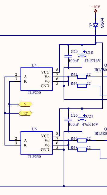
Refer to Taners 2nd or 3rd circuit revision, it shows a correct TLP250 wiring.

It should be corrected this way:
90_1282588270.jpg


Regarding input voltage, the transformer has to be designed for 12 or 24V either, so all other circuit and software details can be selected respectively.

I didnt think about input current while designing PCB.
Obviously. If you want to operate the inverter with a load some day, you should think about, though.
 

FvM in our case inverter output and transformer input is from 6-8 Volts

Added after 3 minutes:

one thing more Fvm how can top two tlp's work under 10 volt???

Added after 3 minutes:

some people successfully tested the circuit if they share there experience and tell about changes they made in circuit it will be helpful for others to make it easily, when then circuit is finalized i'll make a final version of PCB, also if some people can help they can join me.... Thanks
 

Status
Not open for further replies.

Part and Inventory Search

Welcome to EDABoard.com

Sponsor

Back
Top