Continue to Site

Welcome to EDAboard.com

Welcome to our site! EDAboard.com is an international Electronics Discussion Forum focused on EDA software, circuits, schematics, books, theory, papers, asic, pld, 8051, DSP, Network, RF, Analog Design, PCB, Service Manuals... and a whole lot more! To participate you need to register. Registration is free. Click here to register now.

LCRZ-Meter project(DDS signal source), large project with many questions/subjects.

Status
Not open for further replies.
I guess the question is:
How do I control the voltage drop over the bjt in the capacitance multiplier?
 

the resistors are drastically impacting the output voltage in a way I haven't been able to grasp.
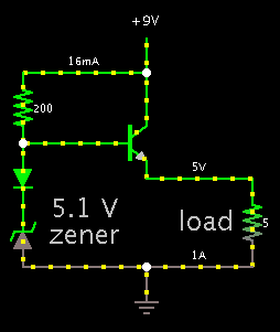
Several resistors probably can be eliminated (or at least reduced in value).
This voltage regulator is the simplest configuration. You may find it is satisfactory.

5550084200_1467351045.png


Notice that bias current flows through the load. Therefore the load's behavior could affect proper regulation. This suggests it is a good idea for you to create individual regulators for all your supplies.
 
  • Like
Reactions: David_

    David_

    Points: 2
    Helpful Answer Positive Rating
Hi,

Don't make the power supply over complicated.

The capacitace multiplier is good for relatively low frequencies and high unexpected currdnt peaks.
(You could use it in sophisticated audio (pre) amplifer curcuits.

But in your case you have expectable output conditions: known frequency, no current jumps, do pulses..

And - for the measurement side - you don't need that extra low noise supplies.
I'd say a standard circuit, maybe folowed by damped LC filters for the analog part is all you need.

Klaus
 
  • Like
Reactions: David_

    David_

    Points: 2
    Helpful Answer Positive Rating
Ok, both sounds as good advice and considering the low/noise regulators available today maybe I'll skip the capacitance multiplier and go with 10000µF bulk capacitors instead.

How about this then, it is probably not strictly necessary but it bugs me to have a positive regulator with 40µVrms noise and a negative one with 600µVrms.
TL1963A(low-noise positive adjustable regulator) is not that expensive, at least it is half the price of really fancy regulators such as TPS7A47/TPS7A33 which is two regulators that is ultra-low-noise regulators.

But is there really anything stopping me from using a TL1963A for the negative rail? simply by connecting the output to the 0V and driving the negative rail with that circuits 0V?
dual_plus_supply.png


The concept is okay as long as the windings have a reasonable balance of power taken from them. Draw too much from one winding, and the other winding drops in output.

Your transformer needs to be a 3-winding type, which may not be easy to obtain. However you could use an ordinary center-tap type, but you need to be able to disconnect wires at the center tap. This may or may not be possible.
 
  • Like
Reactions: David_

    David_

    Points: 2
    Helpful Answer Positive Rating
Actually I have a or I have looked out a transformer to buy that has 3 winding's, if you are referring to 1 primary and 2 identical secondaries?

- - - Updated - - -

But there will be no balance in this case, what the last picture posted are missing are the regulators that create 1*3,3V & 2*1,8V that will be supplying the µC, DDS, and the data-converters. Sure that is not much power we are talking about but still a constantly drawn current/power.

Maybe I can compensate the high-noise negative regulator with some heavier LC-filter than that on the positive rails filter.

Klaus mentioned that my measurement circuits doesn't need that low a noise, but is there any way that I can quantify the level of noise t´with it's impact on the system or is implementing and measuring the circuit the only way to find out?

- - - Updated - - -

I'm sorry to double task the discussion like this, but it is in my mind to be expressed right now.

I have a big problem grasping the actual connection and final structure of the LIA, Klaus dismissed my last attempt at an illustration by pointing out that one of the two channels was connected to 0V thus it vill always be 0V.

But before we go there let me ask you about the structure of the dual-phase LIA, in some illustrations it is obvious that there are 1 reference signal(split into two signals with 90deg phase shift) and 1 input signal that is lead to both Phase Sensitive Detectors(PSD's).

But sometimes I get the impression that the 2 PSD's receive two different signals, the first PSD receives the signal from before the DUT and the second PSD receives the signal from after the DUT. However that presents the problem with the 0V connection.

Is it an amplifier across the DUT that I am missing?
That will extract the voltage drop and pass that along to both of the PSD's?

Like this:
lia.png
One thing the illustration is lacking is the gain stage(s) between the Sine-source and the reference output.
 

Hi,

I see some issues with your circuit.

* You have an amplifier, amplifying the voltage across the DUT. I don't think it is necessary. Or do you expect very low voltages?
* The LPF is at the wrong place. You need an LPF before each ADC.
* Your circuit just measures the voltage across the DUT, but you need the same LIA again for the DUT current.
* The comparator_and_phase_shift needs to be very exact. Any phase jitter and phase deviation will influece the result.
(Therefore -as said beore - best is if the signals are generated digitally by the DDS chip. In my case both, the sine and the phase signals are generated digitally by a FPGA.
On the other hand the high frequency ADC solution needs the same exact treatment)

Klaus
 
  • Like
Reactions: David_

    David_

    Points: 2
    Helpful Answer Positive Rating
Ok now I think I see, but have a couple of questions.

1, The "current LIA" is then supposed to measure the voltage drop over the current setting/limiting resistor right, if you where doing this, would you measure the voltage drop over that resistor differential or would you measure the lets call it range resistor and the DUT and then subtract the DUT voltage measured with the other "voltage LIA"?

2, I don't know straight away how the circuit should look like but I plan to use the DDS IC's internal comparator to convert the sine-wave into a square-wave, as far as I know I will not introduce any error but that action it self, then I have found a presentation of a circuit, the document:
https://www.ti.com/corp/docs/university/pdf/adc2012_politecnico_di_milano.pdf
it is called "Wide Bandwidth 90 Degrees Phase Shifter for Lock - in Amplifiers" and it presents a circuit which uses a opamp/comparator phase shifter that measures the peak voltage at the input and then measures the peak output voltage and then by a feedback-loop adjusts a VGA amplifier to restore the phase shifted signals amplitude.

I did not think that the 90deg phase shift would be as complicated as it appears to be if it is going to perform the task well, I have looked at the components cited in the above document on the last page or which summarizes the hole document, I may as well show it since I made a picture out of it:
90deg_phaseshiftcircuit_50%.png

That is the only largely complete circuit I have found that is advertised as being up to the job, what do you think of this concept?

I've looked at the specified IC's but that VGA seems very tricky to work with, but does the amplitude of the reference spuare-wave matter?
 

Hi,

1)
Both measurement techniques are possible.
I decided to do without an extra amplifier (for the current measurement with shunt).
In either case you should treat both signals very symmetrically.

If you use an amplifier in one path it causes delay/phase shift...then use the same circuit in the other path. So they can compensate each other.
Again: For high quality measurement you need to take care of your signals. Not only the amplitude, but also the phase shift.
With errors in the phase shift you see wrong calculated values for R, L, C.

The signal quality of the LIA output is very high, so there is no big difference whether you do the subtraction before or after the LIA.

2)
The circuit looks sophisticated. Theoretically a differentiator or integrator generate 90° phase shift.
But the one's output amplitude increases with frequency, and the other decreases amplitude. The AGC compensates for that.
So the comparators work at equal operation point. This makes it precise.

The square wave amplitude is not very important. It is just a logic level signal. Look at the analog switch datasheet about specifications.

Klaus
 

As I have said earlier the motivation for this project is in part my wish to create a device like this but the biggest motivator is learning, and phase is one of the major subjects which I am struggling with and don't really get.
In fact I am quite disturbed by realizing how hard I find it to grasp very very basic things and how bad I am at asking the right questions, earlier today I realized that since 1F capacitor charged to 1V can deliver 1A a 100µF capacitor charged to 1V can deliver 100µA.
And if I am dealing with a 3,3v circuit I can grasp how much current each decoupling cap can supply in one discharge by taking 0,1µF = 100nF which translates to 100nA times 3,3 = 330nA...
That I realized today...

1,
I think I would prefer to use a differential amplifier to extract the voltage drop across the current limiting resistor, since the 2 amplifiers need to be identical to cancel each others impact on the system out I will use a differential amplifier for the DUT as well which isn't really necessary since one side of the DUT is connected to 0V.
2 instrumentation amplifiers looks like a viable solution.
What is important for me is the result, and I don't mind resorting to use a more costly type of amplifier in order to create a functioning system that gives good results rather than to make the smart choices and complicate things more than I have to, so as long as I am not choosing a path that has inherent error sources as an affect I am happy.

2,
But I have a hard time thinking about the situation. If that resistor is supposed to limit the current then why measure the voltage drop over it,since it is the limiting factor then I should know the voltage drop.
Or is it the case that I have made a mistake and the circuit does in fact need 1 current limiting resistor and one low value current sense resistor that is used to extract the current signal? But that sounds sort of weird also.

Well I guess that the current limiting resistor functions like setting the lowest possible measured value and the intent is to use current limiting resistor that is always well below the impedance value of the DUT, having written that it seems quite obvious but I can never trust my own deductions.

3,
Do I need two LIA's, one for current and one for voltage, both of which is a "dual PSD LIA"?

I think I am looking at things from the perspective I had started to build in regards to the auto-balancing bridge solution where I measure the current and voltage and extrapolate the phase relationships from the peaks.
I do understand that the 90deg phase shifted reference signal together with a second PSD creates a LIA with two output signals, the first signal with 0deg phase shift reviles the content at that frequency, but the 90deg phase shifted PSD's output what does that give me?
As far as I can comprehend it should provide the same signal but the information is concerning the 2nd and 3rd quarters of the full sine-wave cycle as opposed to the 1st and 2nd that the 0deg reference would give me...

Ok now my lack of insights starts to revile what I have trouble getting, I have two reference signals each with 50% duty cycle.
Am I lost if I think that the first 0deg PSD extracts information of the first half of the sine-wave at it's frequency?

4,
Could someone explain what the 90deg phase shift in the reference signal is supposed to result in?

I have come to understand that a LIA circuit can provide me with information which together with what I already know such as the excitation frequency have all the needed peaces to calculate the complex impedance, and that the LIA is supposed to result in a real value and a imaginary value or magnitudes. I have gone through the concept of complex numbers and phasors and the relationship between the real, the imaginary and the phase value, the real value being the X axis, the imaginary value being the Y axis and the phase value being the angle between the real and the imaginary values or magnitudes. I am not done though.

I will soon concentrate on the 90deg phase shift circuit but until I understand more I'll will let that part rest, oh and just to say, I plan to have the two amplifiers(I and V signal buffers) be identical with a choice of gains. I want gain in order to be able to measure really small values, actually my ambition is to enable as wide a range of impedance as possible and one limiting factor I know of is that at some point the created voltage drop over the DUT is to small to measure and by introducing gain I can thus enable those small Z values to be measured.

By the way, I am not sure what I am trying to do by numbering certain questions. I think I am trying to find a system which easily can show what parts of my texts are most important for me to ask for advice on or I am trying to differentiate between asking questions and reasoning.
I don't know.
What I do know is that I am reading about LIA's but the majority of the information is concerning the same basics which never goes into any of the details I fail to grasp.
 

It's plain you are being very deliberate in your approach, as you design this project. It's commendable, of course. There is nothing wrong with careful planning. However you are uncovering questions, detailed questions, that need to be explored with real equipment, rather than theoretical equipment.

I cannot help thinking somewhere there is a hurdle (at least one) which requires you to experiment with real inductors, attach resistors and capacitors, apply waveforms, watch the oscilloscope, etc. Sessions spent doing these sorts of things at my worktable, I find have been enlightening, as well as a fun and engaging part of my experience with electronics.

Whichever method of measuring you select, it may very well be valid. You have anticipated certain hurdles. However some hurdles pop up only when you are working on real components. I believe that would be a beneficial next step, to test your expectations on inductors of various kinds.
 

Hmm... Sound very reasonable.
For the past couple of day's I have actually been trying to get far enough that I can put together a simplistic version of my system, I have both a Arduino Due with its 12-bit ADC and an Xplained XMEGA A1 board also with 12-bit ADCs, I am working on a USART-PC communication protocol but it is proving difficult but I have already implemented a Arduino Due to Matlab communication that sends streams of the ADCs results in batches of n samples.
Both the Due and XMEGA board does have 12-bit DACs that could be used to generate a sine-wave, the XMEGA have 2 DACs which might be used to generate 1 sine-wave and 1 square-wave synchronized to the same clock.
Then I "only" have to implement some kind of 90deg phase shift circuit and then I would be close to a simplistic version of the system.

Of course I have a Rigol Arbitrary Function Generator... I have not used that for a while.
But the obstacle for me is that if I sit down without a very specific goal or procedure to perform I rarely get anything out of my time spent, that is why I would like to attempt some kind of system that is related to this subject in some way.

It is a difficult situation because I am trying to understand the larger perspective of LIAs and this system but in order to do that I need to answer a few detailed problems, the last day I have been searching for components, the power supply is more or less finished(I will make room on the PCB for additional filters in case they are needed in the end).
I have for a while also been working towards implementing the µC + DDS on a prototype PCB in order to start learning the actual usage of a DDS but then I got into this LIA idea and it appears to me as IF I would grasp the system there isn't really much hardware to put on the PCB.

I think I am also somewhat pressed to get over the my understanding of this system because once I just grasp how the system is supposed to work then I can do all kinds of things on my own and it is then the real work begins.

I just realized that I haven't slept for way to long a duration, so I'll go to bed now and look at this with new eye's tomorrow.

In the mean time I want to thank everyone how has posted in this thread thus far, thank you very much.
 

And if I am dealing with a 3,3v circuit I can grasp how much current each decoupling cap can supply in one discharge by taking 0,1µF = 100nF which translates to 100nA times 3,3 = 330nA...
That I realized today...

The calculation is not accurate.

The recommended way to do: the capacitor is a device that stores charge. The capacitor will be storing a total charge of CxV =0.1*3.3=uC =0.33 uC

This charge can be delivered in 1 sec to give a current of 0.33 uA; but you can also discharge the same in 1us and you can also get a current of 0.33A

Of course the voltage will not stay the same during this discharge but that is a different story altogether.
 

I just realized that I can perform the impedance measurements without the digital circuits and manually take notes on a paper and experiment with the most basic circuit...:)
 

3, Do I need two LIA's, one for current and one for voltage, both of which is a "dual PSD LIA"?.

The short answer is No.

The long answer: Phase is a relative quantity; you need two to have a phase. What we actually do is to use the modulation (AC signal) as a reference. This modulation signal is multiplied with the resulting current signal to get both in phase and out of phase signal.
 

Hi,

3, Do I need two LIA's, one for current and one for voltage, both of which is a "dual PSD LIA"?.
Theoretically you could do with one LIA, as C_mitra says.
But I recommend using TWO LIAs.

To calculate R, L, C you need
* Voltage amplitude at the DUT
* Current amplitude at the DUT
* and the phase deviation of current to voltage.

If I understand c_mitra's solution right, then he assumes the DUT voltage is the same as the signal source signal. In amplitude and phase.
But between the signal source and the DUT you need the current measurement and some wiring. Both will cause voltage drop. Especially at high frequencies even the wiring impedance causes errors.

It depeds on the expected accuracy and how much effort you spend to the software for calibration and error cancelling..if you can go with only one LIA.

Klaus
 

I am really trying to grasp this a quickly as I can because I feel that I have received enough attention for the time being, but I need to get to the point of which I can start and make progress all on my own and I do believe that there is now but one missing peace.

What is the point of phase shifting the reference signal 90deg?

Other than the role of the reference square waves I have a complete picture of the system, that is not to say that I have lots and lots to do and that the software is going to be a real challenge to write but math and software is more possible for me to figure out with reading than this is.

- - - Updated - - -

The role of the square-waves are clear, to be multiplied with the signal of interest and thus in that process extract it from the other frequencies.

But I don't understand the circuit, I have SPICE'ed the circuit Klaus showed of a PSD, the one with two switches driven by the two square-waves and then passed the sine-wave from each PSD along with the square-waves to filters.

I have been driven more and more frustrated with my failure to find the info I seek in documents and now I am asking questions that I would normally feel that I should find out my self and not bother you by, but I have been beaten badly by my inability to maintain my focus and I feel this is no fun no more. Please note that this is expected from time to time and no matter if I find it to be fun or not I will continue to work at it, after some successes it will become fun again, and when things like this are fun you learn much better.
 

What is the point of phase shifting the reference signal 90deg?

I too do not know. Please let me know as I also want to know.

The role of the square-waves are clear, to be multiplied with the signal of interest and thus in that process extract it from the other frequencies.

Square wave does not have all frequencies- only the odd harmonics - see https://mathworld.wolfram.com/SquareWave.html

Higher harmonics are real difficult to extract because their contributions are less. Square waves are equally tough to produce because of the singularities involved. A quadrature detector is best used with sine waves.
 

Hi,

What is the point of phase shifting the reference signal 90deg?
I recommend to do some simple calculations/simulations with excel..

Imagine the psd as an analog multiplier. One input is the sine signal, the other is the logic sqare wave.
When the logic is 1 then the analog signal is multiplied with gain of +1.
When the logic signal is 0 then the gain is -1.

Now have a look at the output of the multiplier.
When sine and square wave are in phase.. then when the square signal is 1 the sine us also in the positive halfwave.
Pos x pos = pos....the output us positive.
When square wave is negative, then the sine is also in it's negative halfwave.
Neg x neg = pos...the output is positve again..
Therefore the result after the filter is positive.

Now imagine the sine is 90° phase shfted. Then there are 4 phases:
Logic = high, sine = neg, output = neg
Logic = high, sine = pos, output = pos
Logic = low, sine = pos, output = neg
Logic = low, sine = neg, output = pos
Filter output = zero.

You can play around with several phase shifts and in the end you will see
* that the output of the non shifted multiplier gives the real part
* and the 90° shifted gives the imaginary part
of an complex vector.

And the complex vector gives the amplitude and the phase of the sine signal. All you need to calculate RLC.

Klaus
 
  • Like
Reactions: David_

    David_

    Points: 2
    Helpful Answer Positive Rating
Thank you, I can't tell you how much that post helped me.

Boy do I really hate google sometimes, how many hour can one spend searching finding crap before one goes mad...

I did find this:
DtypeFlip-Flp_90deg_phase_shifter.png

Which I am hoping is half the solution to the 90° phase shift circuit, all I need to do is to create the comparator circuit that squares the sine-wave. But what my problem is that I can't find a frequency doubling circuit to pair with the flip-flop circuit above.

I find plenty of frequency doubling circuits but everyone of them are not suitable for real use since they have no reliable duty-cycle relationship from input to output and I have a 50% duty-cycle square wave spanning 10Hz to 1MHz and I need a 90° phase-shift. And I thought that I was on the right track but the doubling of that signal into a 20Hz to 2MHz 50% duty-cycle to be feed to the flip-flop circuit above to end up as a phase-shifted 10Hz to 1MHz 50% square-wave signal.

Does any one have any advice on this?
 

Status
Not open for further replies.

Similar threads

Part and Inventory Search

Welcome to EDABoard.com

Sponsor

Back
Top