Continue to Site

Welcome to EDAboard.com

Welcome to our site! EDAboard.com is an international Electronics Discussion Forum focused on EDA software, circuits, schematics, books, theory, papers, asic, pld, 8051, DSP, Network, RF, Analog Design, PCB, Service Manuals... and a whole lot more! To participate you need to register. Registration is free. Click here to register now.

Help re-creating a replica movie prop

Status
Not open for further replies.
You can do all that without the gates, just use a diode from each switch to combine their outputs and a single transistor to invert the result (if necessary) before triggering a monostable. If a 556 (like two 555s in one package) is used, the first can set the beep length and the second make the beep tone.

Brian.
 

Thank you for all the hard work! I can certainly wait a week. I'm just starting to dip my toes soldering the main circuit, which will keep me busy for a long time!
 

Hey Brian!

Thank you for chiming in. I welcome everyone's input and won't be touching this part of the circuit anytime soon. Whatever you guys think is easiest is what I'm looking forward to!

Thanks,
John
 

Hi,


You can do all that without the gates, just use a diode from each switch to combine their outputs and a single transistor to invert the result (if necessary) before triggering a monostable. If a 556 (like two 555s in one package) is used, the first can set the beep length and the second make the beep tone.

Brian.

I really feel that sneer, thanks Brian. Passive-aggressive put down, there? I don't really care anyway, I was just trying to be helpful.

Any schematic or link of what you breezily describe?
 

Absolutely no insult intended whatsoever.

I just wanted to point out that there is a simpler way to achieve the same result. All it has to detect is the presence of a voltage change at any of the switches. As they are all toggle switches to latch the digit data, a diode from each switch would produce one common signal if any switch was operated. OK, it wouldn't detect any switch while another was closed at the same time but that restriction also applies with the logic gate solution too. The diodes make a wired-OR gate without active components being needed.

The dual timer solution is commonplace, one half of the 556 is used in monostable mode to produce a fixed length single pulse and the other half used in astable mode to produce the tone. The output of the first half gates the second half so a fixed length beep is produced.

Brian.
 

Hi,

No offense taken. You could post a schematic for our friend here, 'though, to avoid their accidentally selecting something dodgy trawled out of the murky depths of Internetland... And I agree that your suggestion is far more practical - less parts and flexible r.e. the sound/tone.
 

So if I'm following with my limited knowledge, we can jump power over to the 555 from a toggle with a Diode? Yes, a schematic and layman explanation would be much appreciated!

Thanks!
John
 

Have to leave for a few hours in a moment, I'll draw a schematic for you when I get back. Basically though, think of an NE556 (or two NE555s) to make the beep and one diode from each toggle switch meeting up with it.

Brian.
 

Apologies for the delay - funny how nice simple meetings turn into all day torment.....

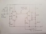
I've sketched the idea I had, I'm pretty sure it is OK but I haven't had time to check it fully:
20181115_205522a.jpg
Sorry about the quality, I hope it is readable. The ICs are NE555 but you can use an NE556 which is a dual version to save one part if you swap the pin numbers for their equivalent functions. The values shown should give a beep lasting about 0.8 seconds at about 800Hz, you can adjust the resistor values to tune the period and tone if necessary.

Brian.
 

Thanks, Brian. I'll try that out.

On another note, I spent two hours tonight attempting to wire one digit on a proto board, but it was a disaster. Got it all wired, but it didn't function at all.

I chalk the problem up to everything being too tiny for my inexperienced hands, and I most likely fried the 4511 at some point. Need DIP sockets for sure.

I'm going to take the time to learn the PCB Express software and have a circuit board made.
 
Last edited:

Hi,

Thanks, Brian. I'll try that out.

On another note, I spent two hours tonight attempting to wire one digit on a proto board, but it was a disaster. Got it all wired, but it didn't function at all.

I chalk the problem up to everything being too tiny for my inexperienced hands, and I most likely fried the 4511 at some point. Need DIP sockets for sure.

I'm going to take the time to learn the PCB Express software and have a circuit board made.

Can you explain a little further? If not, not to worry. If you don't have any multi-coloured wires yet, get a piece of Internet cable (with rigid wires inside) and circuit life becomes far less painful. Maybe you have one of those leads that comes with routers that are about 2m long... Protoboard is soldering board with holes in it, is it?

Do you have a pcb fuseholder and any fast blow fuses (just over the current you expect the circuit to safely see) - helps to avoid accidentally damaging whole circuits or individual parts when inevitable mistakes or accidents happen (connecting V+ and V- backwards, accidentally shorting something or other, etc.).
 

So, I'm certain it's wired properly, by which I mean from power source and thumbwheel to chip, and chip to 7 segment.

However, I hand soldered everything, and definitely spent too much time with the iron pressed against the pins of the 4511 as well as the 7 segment. It's a constant, 30w iron.

Also, and I'm still confused on this, anything that's grounded I just sent to random, unoccupied holes on the proto board. Should I have sent them to an area that is also connected to the ground of the 9 volt??
 

Hi,

Don't worry about cooking ICs, you may not have damaged anything. just quick solder points will do in the future.

And, yes, gnd connections need to go to the supply gnd point on the protoboard, ideally a "star" connection ground.
 

Ok! So maybe if I join all the grounds and jump them over to the battery this actually works.

STILL, it's was too complex for a proto board, at least for me. There is very limited space and everything has to be just right to accommodate the hundreds of components and wires. I'm not skilled enough. I think learning how to use Express PCB and ordering a giant circuit board for all 12 readouts, or 12 individual mini boards will make this project easier for me.

Your thoughts??
 

Agreed, Ground = 0V = All joined together and usually in a digital circuit, the negative side of the battery.

Just a warning about 'Express PCB' and I must state that I do not use them or have any affiliation to them or any of their competitors, they ONLY accept PCB designs made with their own software package. That means you are restricting yourself to a single supplier if you use it. That may be fine for what you need but be careful not to 'corner yourself' if you want to expand your activities in the future.

Brian.
 

Thank you, Brian. Most likely, this will be the only circuit I make for a while, considering it's a replica prop. Also, this one will keep me busy for quite some time. I'm doing pretty well creating the schematic. I assume I must make the schematic represent all 4 digits, not just one, right? I'm depicting all 4 currently.
 

I learned something amazing this evening while working on my circuit board. Component outputs aren't in numerical order, they're all jumbled up, but you have to send those signals out to a destination without ever crossing traces. The restriction of movement can be frustrating, but it forces you to tidy up trace paths, reverse-engineer, work backwards and really think holistically about the board. What I originally thought would be my first position 4511 for the first 7 Segment actually became fourth in line to accommodate traces for the other 3 digits. Crazy, but a lot of fun!
 
Last edited:

I haven't ever used Express PCB myself but generally they expect a complete layout file, in other words a map of the board edges and all the copper traces on it. As you are replicating the same circuit many times, you can probably design the main part once with the displays and driver IC then make multiple copies of it on one sheet of copper board. The layout is really according to you own preference though and you should be careful to accommodate things like mounting screws and of course make sure everything lines up properly when finally assembled.

Designing PCBs is an art, not a science but technical appreciation of what you are trying to do is an advantage. I have seen some REALLY bad designs that are technically correct in that they connect the right things together but for example, overlap the placing of components. I've even seen 7-segment display boards where the rows of pins are so close together that it is physically impossible to mount the display bodies next to each other.

The usual PCB design flow is:

1. draw a schematic
2. Produce a 'net list' from it. This is a file describing which pins are linked together on the components (aka. 'nodes').
3. make sure you have the physical dimensions of the parts and pin positions. These are often in a standard library provided with the software.
4. Draw the PCB outline. This gives you a guide to constrain the parts placement.
5. Place fixing holes and any parts that must be in a particular place.
6. Place all the other parts in sensible positions close to, but not necessarily exactly where they are likely to work best.
7. If you have autorouting available, let it try to find a way to connect the circuit with tracks such that they never cross over each other.
8. For un-routable parts or if you route it manually, create a "rats nest". This is a board with all the connected points joined by straight lines.
9. Move parts around so the tracks are optimized and never cross each other or get too close together.
10. Send the resulting design to the manufacturer. They should return a PCB with copper tracks, drilled holes and placement printing to you.

Be patient - it can take a long time. I've designed PCBs that took weeks of solid time to prepare, and bear in mind I've been doing it for more than half a century!

Brian.
 

I think I made the right side circuit! So, I spent hours drawing circuits last night and learned that boards force you to work backwards, reverse-engineer, and consider work area and usable space, all of which I appreciate as a graphic designer by profession. Since I'm restricted by dimensions of a briefcase this will live in (remember, this is an accurate replica of a movie prop), I didn't have free reign to open up the circuit in any direction. Six of the readouts have to fit on the left side of the case, and six have to fit on the right side of the case. Well, I think I finally created the circuit. I duplicated it five additional times, and all six fit within the dimensions required. Now, I just hope I can get some of the traces in Express PCB as close together as my drawing below (created in Illustrator). I think 7 Segment 3 and 4 have the potential to cause problems. Keep in mind, I'm being faithful to something that already exists, that I've never examined in person, but the readouts now are oriented and align exactly like the movie prop.

Also, for this circuit (which is the only one I'v managed to fit inside the case twelve times), the grounds from all 7 Segments don't have traces, and will be jumped with wire. Also, the 4511 input pins don' have traces and will be hand soldered beneath the board from the Thumbwheel, and out to wherever they head. YES, now I appreciate the existence of Multiplexers, haha!

Below are two images: the first is the finished circuit, including a colored breakout of each 4511 to each 7 Segment. The second is another functioning circuit that is too big to fit all 12 in the case. Now to create the left side circuit, which hopefully doesn't get much larger than the right.


Last edited:

Graphically, that's wonderful but I doubt it would convert to a PCB easily. You have to consider that all the pins on the 4511 have to be connected in the IC pin order as well. I would advise you to download Express PCB or a similar package (I prefer Kicad) and follow the instructions before spending more time with Illustrator as the format it produces will not be compatible with PCB CAD software.

Brian.
 

Status
Not open for further replies.

Part and Inventory Search

Welcome to EDABoard.com

Sponsor

Back
Top