Continue to Site

Welcome to EDAboard.com

Welcome to our site! EDAboard.com is an international Electronics Discussion Forum focused on EDA software, circuits, schematics, books, theory, papers, asic, pld, 8051, DSP, Network, RF, Analog Design, PCB, Service Manuals... and a whole lot more! To participate you need to register. Registration is free. Click here to register now.

Differential probe build

Status
Not open for further replies.
At least two problems:
- still asymmetrical voltage divider by not switching the input side of the negative dividers
- PCB clearance not suited for 2 kV input voltage

Why not single compensated divider strings for positive and negative path?
 

- still asymmetrical voltage divider by not switching the input side of the negative dividers

Fixed that, luckily it's a 4P3T switch.
diff-probe-25.png

- PCB clearance not suited for 2 kV input voltage

I'm using 3KV/mm I understood that would be sufficient?

Why not single compensated divider strings for positive and negative path?
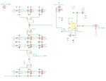
I don't understand your question.

Do you mean :

1. "Why not a single compensated divider string for positive and negative path"
or
2. "Why not a single compensated divider string positive and negative path, for each range"
 

I mean one multitap voltage divider instead of three.

3 kV/mm is a large multiple of the clearance values suggested by safety and PCB design standards. But you don't even have it. Consider that 2 kV also appears at the open switch contacts after the top divider resistors. Means the switch has to be 2 kV rated.

Parallel capacitances of the compensated dividers are unsuitably high for 100 MHz, even 10 MHz bandwidth.
 

3 kV/mm is a large multiple of the clearance values suggested by safety and PCB design standards. But you don't even have it. Consider that 2 kV also appears at the open switch contacts after the top divider resistors. Means the switch has to be 2 kV rated.

Yes 3 kV/mm is not going to win any safety awards. I have 0,8mm=2.400V. And yes the switch is only rated to 500V, but if I want a 3KV rated switch it's too bulky for the current design. In any case my plans are that I will donate this design to edaboard users, as I went through older posts and only one diff-probe design exists and that's with TL071's. So the design files will be made available and builders can modify them to their own liking.

I mean one multitap voltage divider instead of three.

I was not able to get the desired bandwidth with one multitap. And that is related to the below comment of yours.

Parallel capacitances of the compensated dividers are unsuitably high for 100 MHz, even 10 MHz bandwidth.

This I don't get, why and how are the capacitances unsuitably high? You can see it works very good in the simulation and the relative high capacitances makes it very easy to trim them - and they practically eliminates stray capacitances, so why wouldn't it work in a real circuit?
 

For one because low C is a figure of merit for a scope probe. You don't want to load the circuit being measured. Have the lowest C possible.

Second there is no reason you can't get the same bandwidth using a multi-tap divider in a simulation where the switches are ideal. And in real life you don't want to pay for many 1meg resistors and a high voltage switch.
 

For one because low C is a figure of merit for a scope probe. You don't want to load the circuit being measured. Have the lowest C possible.

OK, that one I have overlooked, for the 10n cap across the 1M resistor, the sim says 150A...

Second there is no reason you can't get the same bandwidth using a multi-tap divider in a simulation where the switches are ideal. And in real life you don't want to pay for many 1meg resistors and a high voltage switch.

I really tried, I could do it with two ranges but then the extremes of each range are equally crappy. With three ranges it was impossible, only the middle range would give a reading that was a bit useful.

But I'll give it another try, I learned something in the previous process.

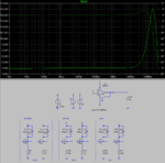
I also took a look at AC analysis as you suggested, it was not daunting as I thought but quite simple, here this one is for you:
Screenshot from 2019-07-15 15-28-09.png
 

For one because low C is a figure of merit for a scope probe. You don't want to load the circuit being measured. Have the lowest C possible.

Second there is no reason you can't get the same bandwidth using a multi-tap divider in a simulation where the switches are ideal. And in real life you don't want to pay for many 1meg resistors and a high voltage switch.

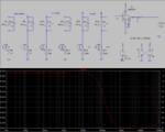
I can't see it happening. This is 0-24V range and there is a 3dB drop, whereas the 240-2400V and 24-240V are ok-ish both have a drop of 0.5dB. If the drop was 0.5dB on all three ranges I could live with that.

Screenshot from 2019-07-15 18-28-12.png
 

First, the suggestion is one series chain per input (positive and negative)

Code:
[in+/-]
  |
[1meg]
  |---------o
[100k]
  |---------o      o--------Amplifier + or -
[10k]
  |---------o
[1k]
  |
[GND]

Second you have different cap values in your sim for the different dividers...decrease the caps and you'll get more bandwidth.
 

First, the suggestion is one series chain per input (positive and negative)

Second you have different cap values in your sim for the different dividers...decrease the caps and you'll get more bandwidth.

Yes, that is what I was trying to illustrate, I can not use same value caps for all three ranges.

I can not find any cap values that will satisfy all three ranges.

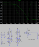
Screenshot from 2019-07-15 19-32-35.png
 

Would this be acceptable by any EE standards? As I said, I can make two ranges work fine, but three ranges - nearly impossible for me. So this is the closest I could get today, and the odd one out is the 0-24V.
phew.png
 

10 pF input capacitance is still large for an active 100 MHz probe but at least acceptable for a number of measurement problems. To realize the bandwidth, the source impedance must be lower than 150 ohms.

The latest simulation shows that off-the-shelf E12 capacitors don't allow a precise compensation. Combinations of multiple capacitors and trimmers are usually required. A real problem arises however if the OP input capacitance is switched between the taps.
 

10 pF input capacitance is still large for an active 100 MHz probe but at least acceptable for a number of measurement problems. To realize the bandwidth, the source impedance must be lower than 150 ohms

The source of what? The diff-amp? The voltage divider?

The latest simulation shows that off-the-shelf E12 capacitors don't allow a precise compensation. Combinations of multiple capacitors and trimmers are usually required.

Yes in reality, but in the sim I can just put in an arbitrary value.

Or do you mean that the correct trimming will be found in the milli-pico's (thousands of a pico).

A real problem arises however if the OP input capacitance is switched between the taps.

That's what I'm doing now, so maybe I should just be content with two ranges.
 
Last edited:

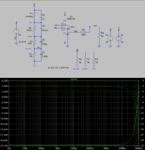
I had a breakthrough with my design, all three ranges +0.5dB@30MHz and +3dB@70MHz.

The breakthrough came when I realized that the dB scale in the AC analysis actually is dBV...duh...

And before you say it's dangerous to switch the gain adjust resistor take a note of this "the differential inputs and the feedback inputs are entirely separate. This means that there is no interaction between the feedback network and the termination network"

Screenshot from 2019-07-19 19-17-46.png
 

Better:
Don't use a BNC for a balanced input, it implies the use of screened cable which will inevitably have more capacitance to the outside World than the center core.
The LED/Zener overload indicator probably won't work because it would take enormous voltage to light them through a 20M resistance or higher. By increasing capacitance across the amp inputs they may also reduce the bandwidth. If you need overload indicators, wiring them to indicate excess output from the amp would be more appropriate and you probably need a monostable to make them light for long enough to see transient voltages.

Brian.
 

Hi Brian.

Don't use a BNC for a balanced input, it implies the use of screened cable which will inevitably have more capacitance to the outside World than the center core.

So how would I determine when to use a screened cable, or capacitance over noise?


The LED/Zener overload indicator probably won't work because it would take enormous voltage to light them through a 20M resistance or higher. By increasing capacitance across the amp inputs they may also reduce the bandwidth. If you need overload indicators, wiring them to indicate excess output from the amp would be more appropriate and you probably need a monostable to make them light for long enough to see transient voltages.

The LED's are relic from when the resistors were 1M and the implementation was simple, I will remove them - I don't want to add extraneous features then I might as well use a MCU, keyboard, display and free cloud storage.
 

So how would I determine when to use a screened cable, or capacitance over noise?
Use two screened cables, ground the shields and use the inners one to each channel. in your present configuration, not only is there a risk of imbalance as mentioned before but the shield is actually half the input so it actually shields nothing anyway.

If you can afford the slight bandwidth trade-off, move the first resistor in the voltage divider to the probe tip so it isolates the capacitance of the cable from the source.

Brian.
 

Use two screened cables, ground the shields and use the inners one to each channel. in your present configuration, not only is there a risk of imbalance as mentioned before but the shield is actually half the input so it actually shields nothing anyway.

No way of denying that. I hear what you are saying, my head started hurting when I looked for a suitable connector, so I kept the BNC because you can get BNC-Banana converter. I will implement your suggestion in V2.0 PRO Edition.

If you can afford the slight bandwidth trade-off, move the first resistor in the voltage divider to the probe tip so it isolates the capacitance of the cable from the source.

Fantastic idea, but likewise V2.0 PRO Edition, I'm getting fed up with this probe build time being, as I said initially I don't want to make a project out of it, I just want to measure - but I ended up with a project as usual, but I learned many new things in the process.

diff-probe-27.pngScreenshot from 2019-07-20 20-11-26.png

Only thing I'm a bit annoyed about is the trimpot that ended up on the scope side, I would have liked to have it on the probe side.
 

Status
Not open for further replies.

Part and Inventory Search

Welcome to EDABoard.com

Sponsor

Back
Top