Continue to Site

Welcome to EDAboard.com

Welcome to our site! EDAboard.com is an international Electronics Discussion Forum focused on EDA software, circuits, schematics, books, theory, papers, asic, pld, 8051, DSP, Network, RF, Analog Design, PCB, Service Manuals... and a whole lot more! To participate you need to register. Registration is free. Click here to register now.

Differential probe build

Status
Not open for further replies.
Why not use fix 1M & 1k and trim them for best CMRR...
and adjust the gain or "differential mode input voltage range" simply with R4?

I tried adjusting the gain x2 and x3, but then the frequency response get's even worse. And for practical reasons the gain would have to be x10 and x100 so I would need a second op-amp as amplifier because AD8130 is optimized for unity gain and AD8129 is optimized for G=10.

And R4 is the reference voltage adjust.
 

Hi,

you want three different setups / ranges.

Can you tell me for each setup
* common mode voltage range
* differential mode voltage range
.. at the probe input.

Klaus
 

Hi,

you want three different setups / ranges.

Can you tell me for each setup
* common mode voltage range
* differential mode voltage range
.. at the probe input.

Klaus

This is what I contemplated before with R6/R9=1K and freq. max 20MHz
Code:
[FONT=Courier New]
R2/R3 C3/C4  DMpp  CMpp
1M    0.016p 4800V 15000V
100K  0.16p  480V  1500V
10K   1.6p   48V   150V[/FONT]
 

Hi,

AD8130 is optimized for unity gain
No. It´s just internally compensated to enable gain down to unity.

But for sure with increasing gain.... bandwidth will be reduced.

***
...then yes, setting the gain with the feedback will not give the expected performance.

Klaus
 

Hi,


No. It´s just internally compensated to enable gain down to unity.

But for sure with increasing gain.... bandwidth will be reduced.

***
...then yes, setting the gain with the feedback will not give the expected performance.

Klaus

I think I found the solution, tell me if this is completely off:

By setting the Cstray value to 10nF the actual stray becomes negligible and Cstray becomes just another capacitor. Then I can set C3/C4 to 100p, and that 100p works with R6/R9 values at 1k/10K/100K (R2/R3 values at fixed 1M)?

- - - Updated - - -

OK, I was confused. with R6/R9 values at 1k/10K/100K (R2/R3 values at fixed 1M), then C3/C4 has to be 10p/100p/1100p. At least there won't be any major issues finding caps for that.

So ranges go

Max DMppMax CMpp
100K/1100p 0-48V144V
10K/100p48-480V 1440V
1K/10p480V-4800V14400V
 
Last edited:

Hi,

every added capacitor has tolerance, too.
You need to calibrate them very precisely ... in either case, to get good HF CMRR.

Klaus
 

Every topology has pros and cons but my suggestion is that you don't implement ranges by changing R6/R9. See how I drew the schematic a few posts ago. The 10K and 2K are always in circuit. The switch selects which node goes into the amplifier.

Then by placing your dominant filter caps right after the 1meg resistor you'll have equal bandwidth for all ranges.

When it comes to matching look at resistor and capacitor networks. Search "ACAS", LT5400, and "X2Y" on digikey to see what I'm talking about. You'll need to calibrate the 1meg's buy maybe not other R's and C's if you choose these networks carefully.

Yes you are right, it's time to compromise, I can't get what really want, so the next best thing is it.

I choose then only two ranges 0-240V and 240-2400V 0-20MHz and this is what I get
Screenshot from 2019-07-08 14-43-37.png

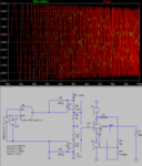
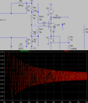
The 0-240V is pretty flat over 0-20MHz, but the 240-2400V has some attenuation (see above trace) which I can't get rid of. But at least it can be trimmed by C1/C2 and there are timmers available for that.
 

Nice trick to see the frequency response in the time domain but I suggest you take a look at LTSpice's AC simulation ability at this point...

I'm wondering how there is a difference in gain flatness. Did you change the input amplitude to make sure you tested both ranges at the same nominal output amplitude?

Maybe the simulated input parasitic s of the amplifier are doing it. If so adding an impedance matching resistor between the 1k's and the amplifier input of 8k should match it to the 9k range.
 

Nice trick to see the frequency response in the time domain but I suggest you take a look at LTSpice's AC simulation ability at this point...

I know, but I was lazy and I know I could do it this way.

I'm wondering how there is a difference in gain flatness. Did you change the input amplitude to make sure you tested both ranges at the same nominal output amplitude?

Maybe the simulated input parasitic s of the amplifier are doing it. If so adding an impedance matching resistor between the 1k's and the amplifier input of 8k should match it to the 9k range.

Well, I stopped simulate the parasitic by increasing C1/C2 so the parasitic is negligible in relation to C1/C2, and then C1/C2 can easier be trimmed in relation to C3/C4.

Anyway tried with a resistor as you suggested, and what happened was that for any value of resistance the thing attenuates even steeper.
 

The AD8130 model may have some parasitics.

To be clear the 8k should only be in series with the amplifier inputs when the 1k resistor is selected.

If it 'works' the amplitude rolloff should match between your ranges. Point being you will never be able to properly trim C1/C2 if the two ranges don't match.
 

I have come to the conclusion that the AD8130 sucks above 10MHz. So I changed to AD8131 which is straight as an arrow up to 40MHz and thereafter up to 100MHZ straight as an moist arrow, but still an arrow.

The problem with the AD8131 is that it has a differential output and I would like to convert it to single ended by e.g. a AD8045, but I can't figure out how to configure AD8045 as an differential amplifier?

Screenshot from 2019-07-09 22-27-20.png
 

Pintek DP-15K is rated 35MHz and 15kVpp differential, and 7.5kV common-mode, 100mV 50MEG input. From 15kV down to 1kV at 30MHz.
It uses two THS4631 for their I/P stage op-amps 325MHz FET input. Many compensation capacitors.
Maybe look at their probes to confirm what your requirements are for this project.

Your Spice sim has oddball huge capacitors to GND 192nF on the input circuit, I would not expect it to work at high frequencies.

On the Pintek, the THS4631 was exactly what I was looking for among the Analog products but couldn't find. And I found this too, maybe I will try it http://e2e.ti.com/support/amplifiers/f/14/t/736743

Reg. the oddball caps, I'm glad you noticed. The story is; in the beginning the C1/C4 was only there to simulate parasitic capacitance of 10p and to compensate for that C2/C4 was placed. But I found out there was a 100:1 relationship between so with C1/C4=10p I would need C2/C4=0.1p and to trim a 10p or 0.1p capacitor is difficult, so I simply increased C1/C4 to 100n and thought I could trim by adding caps on top of the 0805 SMD's.
 

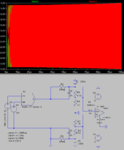
OK, an apology is due to Analog and their AD8130, it doesn't suckk (remove the last 'k') - it was me who sucked. So here it is from 0-100MHz

Screenshot from 2019-07-11 15-38-27.png
 

I made a PCB layout for the signal part (no power-supply) of my diff-probe, are there any RF-aficionados out there that could take a look at it and let me know my mistakes? I didn't want to make it too small and too tight as I'm going to hand solder, and the caps C2/10/13/14/17/18 will need to be trimmed by piggyback-ing smaller value caps, maybe 1-2 additional caps.

diff-probe-22.png

PS if you are a noob like me, did you notice that you make less mistakes now that the regular edaboard experts are on holiday?
 

I don't recognize a differential probe circuit. Previous post #76 looks better.

You have insufficient PCB clearance and the range switch is hardly suited for claimed 2kV. The usual solution found with the differential probes quoted in this thread (Pintek, Testec) is not to switch the top side of the voltage divider.

A true differential probe is expected to a have a fully differential voltage divider and range switch.
 

I don't recognize a differential probe circuit. Previous post #76 looks better.

I couldn't recognize it either the day after, I believe it was a case of LUI.

You have insufficient PCB clearance and the range switch is hardly suited for claimed 2kV. The usual solution found with the differential probes quoted in this thread (Pintek, Testec) is not to switch the top side of the voltage divider.

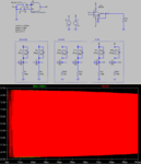
Switched to low side switching...

diff-probe-23.png
 

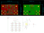
And here is the new and improved layout
board-layout-24.png
The new switch took some more real-estate, and there is more spacing.
 

Status
Not open for further replies.

Part and Inventory Search

Welcome to EDABoard.com

Sponsor

Back
Top