Continue to Site

Welcome to EDAboard.com

Welcome to our site! EDAboard.com is an international Electronics Discussion Forum focused on EDA software, circuits, schematics, books, theory, papers, asic, pld, 8051, DSP, Network, RF, Analog Design, PCB, Service Manuals... and a whole lot more! To participate you need to register. Registration is free. Click here to register now.

Differential probe build

Status
Not open for further replies.
Hi,

I doubt a DVM is the correct instrument to measure isolation.
It was no isolation measurement, just voltage.
...and hopefully it helped to see the problem of your circuit

Klaus
 

They're not your zeners they're the ESD protection diodes inside the AD8130 that result in the "Input Voltage (Any Input) −VS − 0.3 V to +VS + 0.3 V" absolute maximum rating (with the diodes having a 0.3V drop)

Note that the datasheet doesn't explicitly diagram them but I assure you they're there. And even if they're not its even worse: the inputs would have NO protection. With the diodes the you can assume the input pins will survive 5-20mA or or so.

If there are ESD protection diodes inside the AD8130 then you are obviously right. The thing is, it' speculation - but you bring up a valid argument, the 0.3V voltage drop warrants further investigation and I will measure the AD8130 when I buy some. Then I will let you know.

I any case I believe your scenario could be eliminated by placing a diode J3 pin2, but would I then need to lower the ref voltage of U1 equal to the voltage drop of that diode?

- - - Updated - - -

Hi,
It was no isolation measurement, just voltage.
...and hopefully it helped to see the problem of your circuit

Yes and No.

Yes because we have been full circle with what can happen with my circuit if.... and that is a very good exercise.

No because I know there are "voltages" everywhere, but that is a extremely complex matter and there is no way anybody can make the perfect circuit or measurement, so it all boils down to belief systems. Personally in the 30 years I have handled ESD sensitive devices, I have only done so with my bare hands, and never not even once have I had a malfunctioning device because of my (according to some) careless behavior.

Secondly the only instrument I would trust to make such voltage measurements you suggested, would be a electrostatic voltmeter (also on my build list).
 

Again it doesn't matter whether there are clamping diodes or not inside the AD8130. The clamping diodes only act when the input pins exceed the absolute maximum ratings. Either the diodes are there to provide some protection or they're not and there is zero protection. But they're a good illustration of the point: When you drive more than 18V between two of your differential scope grounds (or 9V above scope ground) either those diodes conduct or the absolute maximum is exceeded.


The solution is what both myself and Klauss have said....:
"Thus you (sadly) need a (high ohmic) relation to your GND."

Not only does this add impedance to the problem path but a proper differential circuit is ideally designed to be completely symmetrical. Just copy your selectable high impedance input circuit twice.
 

I sincerely can't understand the way you are trying to communicate. I'm talking about communication, not electronics

Again it doesn't matter whether there are clamping diodes or not inside the AD8130.

How "again"? you mentioned clamping diodes for the first time in thread #37 and there you said they presented a problem or at least that's how it came over, and now they are not a problem(?)

And that's how I generally perceive your communication style, you make a statement be it true or false, then I pose questions which you ignore or you reply with yet another statement very rarely with any supporting arguments or "trust me I know what I'm talking about"-kind of thing. I understood the argument you made in #37, but then you subsequently say "it doesn't matter" so why did you mention it in the first place(?) and we are back to square one. That really does not inspire confidence with me, I'm not saying you are deliberately trying to mislead me or that you don't know what you are talking about, I'm saying: Your communication skills definitely needs an overhaul in my opinion only, because it is difficult for me to take in what you are trying to communicate.

So I mean no personal offense, and I would really wish to hear what you have to say, but your communication style is posing me some real problems. It's not a matter of being right or wrong, I don't mind being wrong and corrected and learn new things, but I had my fair share of air-heads and con-artists (not saying you are one) who uses approximately same communication style, so it doesn't sit well with me.

The solution is what both myself and Klauss have said....:
"Thus you (sadly) need a (high ohmic) relation to your GND."

Not only does this add impedance to the problem path but a proper differential circuit is ideally designed to be completely symmetrical. Just copy your selectable high impedance input circuit twice.

Ok, back to electronics. I think I will abandon this build now because I simply don't understand it. e.g how are resistors or zeners on the input pins of U1 going to prevent the scenario you are depicting in #37(?) And now I just noticed an oversight of mine #19 "Additionally, you must add a trim capacitor to frequency compensate your dividers, otherwise the stray capacitance will form a low-pass filter. " how is additional capacitance then going to increase the cutoff frequency(?) Or "But to calculate this you need to specify the voltage at the floating probes. What is the highest expectable voltage on a floating node w.r.t. EARTH GND?" - How would I know what to expect when "floating" and "isolated" apparently means it's in relation to earth, then it could be any voltage.
 

Ok and from my perspective you understand everything except the conclusion. I try repeating the conclusion and you call me a broken record. So I try a different angle.

The diodes illustrate the relationship you've set up between grounds which is the important point. If you can see the diodes conduct when U1 pin 8 exceeds the rail what stops you from seeing that if they're not there U1 pin 8 will just burn up from exceeding its specification?


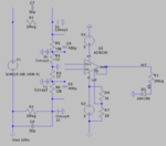
Anyway the way to understand all this is to simulate. Can my circuit withstand large voltages between input GND and scope ground? Add a voltage source and see. This picture shows that and the symetric divider network I've been describing. A DPDT switch could select the 2k or the 10k nodes to send to the amplifier for 2 range choices. In this case V9 (common mode) is 10Khz while V8 (differential) is 1khz. If the circuit is working we'll only see the differential signal at 1khz. And it does:

That type of symetric divider network where you divide the (-) equally to the (+) is all you need.


The C you're asking about would go in parallel to R3/R8 to act like a high pass filter. Google "scope probe compensation".

You probably don't know the exact differntial voltage you'll encounter either but that didn't stop you from picking something. Your probe will have a common mode limit too. Most important: know what it is. See this probe specifies "-Up to +1400V (DC +Peak AC) Differential and Common Mode". Every differential probe has a common mode limit, usually about the same as the differential one.
https://probemaster.com/4231-differential-probe-1-20-200-25-mhz-1400v/
 

Attachments

  • Capture2.PNG
    Capture2.PNG
    35.3 KB · Views: 132

Hi,

The circuit in post #45 shows the problem (V9) as well as the solution (voltage divider to GND).

Klaus
 

Ok and from my perspective you understand everything except the conclusion. I try repeating the conclusion and you call me a broken record. So I try a different angle.

OK I understand what you are saying, in communication, if a person understands everything except the conclusion it is obvious that there is a missing argument in the line of reasoning you are trying to communicate. So simply repeating the conclusion without the missing link is counterproductive. Then you try a different angle which is a valid approach, but when you change the angle from message to message then you appear (not saying you are) uncertain in what you are trying to communicate. And may I suggest that when it appears to you that I'm not understanding e.g. when you encounter a question, do not immediately jump to a different angle but try to address the point being raised, this could uncover the missing link.

The diodes illustrate the relationship you've set up between grounds which is the important point. If you can see the diodes conduct when U1 pin 8 exceeds the rail what stops you from seeing that if they're not there U1 pin 8 will just burn up from exceeding its specification?

It's not that I don't see it, it's just that it doesn't raise any severe concerns with me because I'm not the worrying type, not necessarily for a technical reason. But I can be convinced by technical reasoning e.g. your post #37 and also in #45

Anyway the way to understand all this is to simulate. Can my circuit withstand large voltages between input GND and scope ground? Add a voltage source and see. This picture shows that and the symetric divider network I've been describing. A DPDT switch could select the 2k or the 10k nodes to send to the amplifier for 2 range choices. In this case V9 (common mode) is 10Khz while V8 (differential) is 1khz. If the circuit is working we'll only see the differential signal at 1khz. And it does:

That type of symetric divider network where you divide the (-) equally to the (+) is all you need.

Thank you, this I understand and I will try the simulation.

The C you're asking about would go in parallel to R3/R8 to act like a high pass filter. Google "scope probe compensation".

Thank you, I can understand that.

You probably don't know the exact differntial voltage you'll encounter either but that didn't stop you from picking something. Your probe will have a common mode limit too. Most important: know what it is. See this probe specifies "-Up to +1400V (DC +Peak AC) Differential and Common Mode". Every differential probe has a common mode limit, usually about the same as the differential one.
https://probemaster.com/4231-differential-probe-1-20-200-25-mhz-1400v/

OK, all clear now. The missing link in my case was that "isolated" sometimes imply "earth"-lyish connection from a engineering perspective.
 

OK, all clear now. The missing link in my case was that "isolated" sometimes imply "earth"-lyish connection from a engineering perspective.

Glad a lot of it is cleared up.

When it comes to ground I say this: "There is no ground".

Any two nets have some relationship in terms of voltage, impedance etc but whether they have 'ground' in their name or not tells you absolutely nothing about that relationship. Better to treat them as net A and net B and draw the schematic relationship between them.

This is particularly important when you get into high voltage, isolated and differential circuits like this one where there really is "no (single) ground"
 

I made the simulation, and it was actually the most interesting op-amp sim I have ever done (haven't done many though) and it worked! As for maximum common mode voltage on the probe input I'm thinking 2-3KV.

Screenshot from 2019-07-06 20-58-34.png

The only complaint I would have is that gain slightly rises with input frequency and I don't know how to counter that. And the other thing is that I can only adjust the voltage divider by adjusting R9 and R6, but that's not a complaint.

And here is a medal for asdf44 who has earned it for his patience with me.
patience44.png

This is a gift for KlausST that he can use at his own discretion on this forum.
approvalST.png

For some reason I can't attach .cir .asy and .asc file for LTSpice, so I added the .txt extention. Remove that if you are going to use these files.
 

Attachments

  • diff-probe.asc.txt
    4.2 KB · Views: 92
  • AD8130.asy.txt
    817 bytes · Views: 93
  • ad8130.cir.txt
    2.5 KB · Views: 109

C stray should be more like 10p probably. You might only need a 1pF or less across the 1megs.

What are the 12 ohm resistors, that's tiny?

Be careful with resistor selection: Resistors have voltage limits as well as power limits. 2-3kV requires very special resistors or should be implemented with many resistors in series (1206 resistors will be rated for 100-500V or so).

Precision is also very important, not for gain accuracy which is easy to calibrate but for common mode rejection (simulate one divider leg being 10% off, set your differential voltage source to 0 and add a common mode source to see for yourself). This is one reason differential probes are expensive: because precision high voltage resistors aren't cheap.
 

Hi,

R6, R9 need to be as high value as possible to get best precision and best common_mode_rejection.

For 3000Vp I recommend to go close to full 7.5Vp (useful common mode input range of Opamp)
This means up to 2500 Ohms ... for 1MOhms input resistors.
This still is a ratio of 400:1.

Thus you need less gain in the Opamp .... and thus gain will be more flat .... and upper cutoff frequency will be higher.

Klaus
 

For 3000Vp I recommend to go close to full 7.5Vp (useful common mode input range of Opamp)
This means up to 2500 Ohms ... for 1MOhms input resistors.
This still is a ratio of 400:1.

That's not how it works in the sim, the highest I can go R6/R9 is about 1K without distortion.

Screenshot from 2019-07-07 11-12-47.png

C stray should be more like 10p probably. You might only need a 1pF or less across the 1megs.

Noted.

What are the 12 ohm resistors, that's tiny?

See above.

Be careful with resistor selection: Resistors have voltage limits as well as power limits. 2-3kV requires very special resistors or should be implemented with many resistors in series (1206 resistors will be rated for 100-500V or so).

Precision is also very important, not for gain accuracy which is easy to calibrate but for common mode rejection (simulate one divider leg being 10% off, set your differential voltage source to 0 and add a common mode source to see for yourself). This is one reason differential probes are expensive: because precision high voltage resistors aren't cheap.

Farnell has 1% 2512 SMD 3KV resistors at about €1,5 and MELF costs about the same.
 
Last edited:

Hi,

I talked about "common mode", but you simulated "differential mode"
According datasheet differential mode input voltage range is +/-2.5V.

Thus distortion is expectable.

Klaus
 

Farnell has 1% 2512 SMD 3KV resistors at about €1,5 and MELF costs about the same.

1% is pretty poor. Simulate the common mode rejection with a 1% mismatch.

If you're on budget and just building a couple maybe you can match them yourself...
 

I talked about "common mode", but you simulated "differential mode"
According datasheet differential mode input voltage range is +/-2.5V.

Thus distortion is expectable.

Yes of course.. silly me.

Let me ask this way, what is the min R6/R9 value? Because the sim works even down to 1ohm.

If I decide to maintain e.g. 1k for R6/R9, and choose 1M for R2/R3 I get a 1000:1 ratio which is more practical when measuring, than a 400:1 ratio. That all works fine at 100KHz, but if I increase frequency to 20MHz then C3/C4 starts to play a considerable role. Then I need 0.016p for C3/C4, is that at all practically feasible to trim a cap to 0.016p?

Here are some considerations for different values for R6/R9 at up to 20MHz
R2/R3 C3/C4 DMpp CMpp
1M 0.016p 4800V 15000V
100K 0.16p 480V 1500V
10K 1.6p 48V 150V

With a DP3T slide switch it would be selectable.

Screenshot from 2019-07-07 16-00-58.png

1% is pretty poor. Simulate the common mode rejection with a 1% mismatch.

If you're on budget and just building a couple maybe you can match them yourself...


Yes I'm on a budget, so I will try the DIY matching option.
 
Last edited:

Hi,

MIN value makes no sense in my eyes, because it makes performance worse.
I recommend to optimize in direction "better performance" --> Higher resistance value.

Klaus

With lower value resistance you attenuate the signal even more, thus it needs to be amplified afterwards with higher gain.
Higher gain, means higher noise, higher distortion, higher offset voltage, less common mode rejection, less frequency response...at the output.
 

MIN value makes no sense in my eyes, because it makes performance worse.
I recommend to optimize in direction "better performance" --> Higher resistance value.

OK, if I do like this then: Keep R2/R3 at 1M and switch between 1K/10K/100K for R6/R9 values, then at 20MHz C3/C4 has to switch between values 0.016p/0.16p/1.6p - is that practically feasible to trim caps to such precise values?
 

Look at the frontend of a Testec SI9001 probe, 4 + 4 Mohm input resistance. Separate LF and HF CMRR adjustment.

10270002.jpg

Also attached the CMRR calibration procedure.
 

Attachments

  • SI-90012 Calibration.pdf
    552.8 KB · Views: 142

Hi,

OK, if I do like this then: Keep R2/R3 at 1M and switch between 1K/10K/100K for R6/R9 values, then at 20MHz C3/C4 has to switch between values 0.016p/0.16p/1.6p - is that practically feasible to trim caps to such precise values?
Difficult.
Look for capacitive trimmers. The selection tools and the datasheets will tell you.

***
Another approach.
Why not use fix 1M & 1k and trim them for best CMRR...
and adjust the gain or "differential mode input voltage range" simply with R4?

The circuit becomes more simple and also the calibration...
But you need to check whether the performance is sufficient for you.

Klaus
 

Status
Not open for further replies.

Part and Inventory Search

Welcome to EDABoard.com

Sponsor

Back
Top