Continue to Site

Welcome to EDAboard.com

Welcome to our site! EDAboard.com is an international Electronics Discussion Forum focused on EDA software, circuits, schematics, books, theory, papers, asic, pld, 8051, DSP, Network, RF, Analog Design, PCB, Service Manuals... and a whole lot more! To participate you need to register. Registration is free. Click here to register now.

Boost Converter analysis

Status
Not open for further replies.
Heyyy... new thing for me. wait a second. let me understand this point.
If I reduce the voltage amplitude to the MOSFET then I can lose the efficiency. And also, the MOSFET will not work as a switch anymore, it will work as resistance instead. Is it?
And if I want to retain the efficiency of the Boost Converter then I should reduce duty cycle not voltage amplitude. Did I understand right?

Thank you very very much. so helpful posts.

- - - Updated - - -

I have reduce the duty cycle.
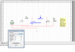
Here is my simulation then. I just reduce the duty cycle to 53% from 76% and removed the series limiting resistor of 0.4ohm.
Capture.PNG

I have gotten what I want. I am getting Vout=5.2v and Iout=500mA.

Now I want to know is there any precaution which I should remember like MOSFET heating or something like that?

Also, I want to know why reducing duty cycle didn't affect too much at the output voltages. But it affect the output current. I have heard from someone that the increasing duty cycle will increase the on time of the MOSFET and the long the MOSFET will conduct (means on time) the more the efficiency. Is it not true at all. huh?
 

Heyyy... new thing for me. wait a second. let me understand this point.
If I reduce the voltage amplitude to the MOSFET then I can lose the efficiency. And also, the MOSFET will not work as a switch anymore, it will work as resistance instead. Is it?

Yes, normally the aim in this topology is to drive the mosfet/transistor as a switch (that is, drive it to its minimum ON resistance).

And if I want to retain the efficiency of the Boost Converter then I should reduce duty cycle not voltage amplitude. Did I understand right?

Correct.

Now I want to know is there any precaution which I should remember like MOSFET heating or something like that?

Yes, check for components overheating under various operating conditions:

no load
light load
heavy load
etc.

The easy way for me to test is by holding components between my fingers. If it is too hot to keep my fingers on, then it needs heatsinking, or else the circuit needs adjusting, etc.

Also, I want to know why reducing duty cycle didn't affect too much at the output voltages. But it affect the output current.

If the load is a resistance, then changing output A will also change V. (That is, if you are not regulating the output.)

I have heard from someone that the increasing duty cycle will increase the on time of the MOSFET and the long the MOSFET will conduct (means on time) the more the efficiency. Is it not true at all. huh?

I'm not sure how much this would affect efficiency in and of itself. There are factors that depend on the specs of your coil, how to get the best performance out of it, etc.

If you can succeed at minimizing parasitic resistances, then you have gone a long way toward obtaining maximum efficiency.
 
  • Like
Reactions: Eshal

    Eshal

    Points: 2
    Helpful Answer Positive Rating
Yes, normally the aim in this topology is to drive the mosfet/transistor as a switch (that is, drive it to its minimum ON resistance).
And we drive the MOSFET switch to its minimum ON resistance if we reduce the Duty Cycle or if we reduce amplitude of voltage of the MOSFET Switch. Right sir?

Yes, check for components overheating under various operating conditions:

no load
light load
heavy load
etc.

The easy way for me to test is by holding components between my fingers. If it is too hot to keep my fingers on, then it needs heatsinking, or else the circuit needs adjusting, etc.
Yes sir, I will surely try it in real life. But before I will attenuate its frequency which is included in the output DC voltage. See my figure in post#61 there is a frequency in the output. It is f=100KHz. Did you see? It is a boost converter (its input is DC and output is DC) so it should not have frequency at the output. So I have thought to use a PI-filter or L-filter in order to attenuate this unwanted frequency. By the way, I want to ask you sir, which filter is good to use so that my efficiency could not be reduced. PI, L or else?

If you can succeed at minimizing parasitic resistances, then you have gone a long way toward obtaining maximum efficiency.
I have learned about the parasitic capacitance but not resistance. I will read about it and then ask you question regarding with this.

I am very thankful to you that you have helped me through out this project. You are so sweet :p

Thank you sir.
 

And we drive the MOSFET switch to its minimum ON resistance if we reduce the Duty Cycle or if we reduce amplitude of voltage of the MOSFET Switch. Right sir?

No, instead the mosfet needs a greater volt amplitude at the gate, if we want minimum 'On' resistance. (We're talking about enhancement-mode mosfets here, not depletion-mode.)

Duty cycle is a different concept from 'On' resistance.

Normally we want to have minimum 'On' resistance in the mosfet switch, whatever length of time it is switched on.

Yes sir, I will surely try it in real life. But before I will attenuate its frequency which is included in the output DC voltage. See my figure in post#61 there is a frequency in the output. It is f=100KHz. Did you see? It is a boost converter (its input is DC and output is DC) so it should not have frequency at the output. So I have thought to use a PI-filter or L-filter in order to attenuate this unwanted frequency. By the way, I want to ask you sir, which filter is good to use so that my efficiency could not be reduced. PI, L or else?

My simulation shows that your ripple is several percent, with the 7.5uF smoothing capacitor in your schematic.

You can reduce ripple by increasing the Farad value. Example, you'll get 2% ripple by increasing the capacitor to 30uF.

The capacitor has several hundred mA going through it, back and forth, each cycle. If you find that a single capacitor gets hot, then you may want to divide the load across 2 or more caps.
 
  • Like
Reactions: Eshal

    Eshal

    Points: 2
    Helpful Answer Positive Rating
No, instead the mosfet needs a greater volt amplitude at the gate, if we want minimum 'On' resistance. (We're talking about enhancement-mode mosfets here, not depletion-mode.)

Duty cycle is a different concept from 'On' resistance.

Normally we want to have minimum 'On' resistance in the mosfet switch, whatever length of time it is switched on.
Got it sir.

My simulation shows that your ripple is several percent, with the 7.5uF smoothing capacitor in your schematic.

You can reduce ripple by increasing the Farad value. Example, you'll get 2% ripple by increasing the capacitor to 30uF.

The capacitor has several hundred mA going through it, back and forth, each cycle. If you find that a single capacitor gets hot, then you may want to divide the load across 2 or more caps.
OK sir, I try with some higher value.
And 2 or more capacitors in parallel. Huh??
Also, you have provided a link to the falstad simulation website. There are ready made circuit. Can't we draw our own to see the current flow?

Thank you.
 

Also, you have provided a link to the falstad simulation website. There are ready made circuit. Can't we draw our own to see the current flow?

Thank you.

Yes. My post #45 gave a link that will:
1) open the Falstad.com website,
2) load my boost converter schematic (battery charger version) into Falstad's simulator, and
3) run it on your computer.

Below is a link that will do the same with my simulation of your post #61 schematic (with slight modifications):

https://tinyurl.com/m2v89xx

You can alter values at will by right-clicking a component, and select Edit.
 
  • Like
Reactions: Eshal

    Eshal

    Points: 2
    Helpful Answer Positive Rating
Hello sir, I have changed the value of capacitor from 7.5uF to 30uF. And I have the significant difference in Vp-p Voltages. Here is picture.
Capture.PNG

But again I want to ask you. It is a DC to DC converter. then why it has frequency 50KHz at the output (in the yellow probe's tag, in the last Freq.: 50.0 kHz)
MOSFET switch frequency is 50KHz. Is it due to this? Should it not be reduced to 0Hz because it has DC output that's why it should be 0Hz signal. Are you getting sir what I am trying to deliver you?

Yes. My post #45 gave a link that will:
1) open the Falstad.com website,
2) load my boost converter schematic (battery charger version) into Falstad's simulator, and
3) run it on your computer.

Below is a link that will do the same with my simulation of your post #61 schematic (with slight modifications):

https://tinyurl.com/m2v89xx

Yes, I have tried. But again I have same question, I want to draw my own circuit on Falstad's simulator. Is it possible? Not the one ready made which has just to change the values for modification. I want to create whole circuit on Falstad's simulator.

Thank you.
 

But again I want to ask you. It is a DC to DC converter. then why it has frequency 50KHz at the output (in the yellow probe's tag, in the last Freq.: 50.0 kHz)
MOSFET switch frequency is 50KHz. Is it due to this? Should it not be reduced to 0Hz because it has DC output that's why it should be 0Hz signal. Are you getting sir what I am trying to deliver you?

By turning the mosfet fully on or fully off, we cause it to carry high current, yet without creating a resistive drop across it. The resistive drop method generates heat and wastes power.

By chopping the plain DC into pulsed DC, we can use it to operate a circuit that converts its volt level to another volt level.

We turn it on and off at a frequency which gets the best performance out of the components.

Yes, I have tried. But again I have same question, I want to draw my own circuit on Falstad's simulator. Is it possible? Not the one ready made which has just to change the values for modification. I want to create whole circuit on Falstad's simulator.

Thank you.

To select which component you will place, right-click on an empty area, and select your desired component.

To clear the canvas, go to the Circuits menu and select Blank Circuit.

To save your circuit, go to the File menu and select Export. A window appears containing text. Copy the contents to the clipboard, paste it into a separate text processor (example, Wordpad). Then save it to disk.

To load a circuit file into the simulator, you must first open it in the text processor. Copy the text to the clipboard. Then switch to Falstad's simulator, select Import. An empty window appears. Paste the clipboard contents into the window, and click Okay.
 
  • Like
Reactions: Eshal

    Eshal

    Points: 2
    Helpful Answer Positive Rating
By turning the mosfet fully on or fully off, we cause it to carry high current, yet without creating a resistive drop across it. The resistive drop method generates heat and wastes power.

By chopping the plain DC into pulsed DC, we can use it to operate a circuit that converts its volt level to another volt level.

We turn it on and off at a frequency which gets the best performance out of the components.
I have gotten your words sir.
I am very very grateful to you for helping me in this thread. I will show my calculation now. Then guide further.
I am very happy that I have done it and it is my first made circuit with your help.

To select which component you will place, right-click on an empty area, and select your desired component.

To clear the canvas, go to the Circuits menu and select Blank Circuit.

To save your circuit, go to the File menu and select Export. A window appears containing text. Copy the contents to the clipboard, paste it into a separate text processor (example, Wordpad). Then save it to disk.

To load a circuit file into the simulator, you must first open it in the text processor. Copy the text to the clipboard. Then switch to Falstad's simulator, select Import. An empty window appears. Paste the clipboard contents into the window, and click Okay.
It is really a very very good simulator. It shows a current flow which help me to understand the working of the circuit. I am wonder if it has UJT too.

Thank you :)
 

Sir, I am doing calculation again for my boost converter.

Besides these, I need to know that as I have changed capacitor 7.5uF to 30uF as per your saying. I observe the significant reduction in the Vp-p voltage from several millivolts to approx. 176mV as shown in the figure in post#67.
But 176mV still shows that output has ripple content. So what should I do if I want to get 0 ripple? Should I increase the capacitor value, if so then capacitor will be much huge for this case. Isn't it sir?

Thank you.
 

To decrease ripple use good design with low pass filter on switcher output.

250px-1st_Order_Lowpass_Filter_RC.svg.png


https://en.wikipedia.org/wiki/Low-pass_filter

One of disadvantage of switcher is ripple voltage and spikes, and to keep this in some acceptable ranges you need to have good design and often additional filtering. Its very hard to get 0V ripple.


Best regards,
Peter
 
  • Like
Reactions: Eshal

    Eshal

    Points: 2
    Helpful Answer Positive Rating
Thank you for your reply sir.

I also thought to use low pass filter. But I am unable to find any design formulas and theory. PI-Filter and L-Filter are also low pass filter. Can't we use these two instead of the one you shown in the post#71?

Thank you.
 

oooo... thank you. finally i have some theory on pi-filter.
But there is not any formula to assist me in designing. how to start designing the simple pi-filter?
 

oooo... thank you. finally i have some theory on pi-filter.
But there is not any formula to assist me in designing. how to start designing the simple pi-filter?

Reduce the time You spend writing formulas on papers and simulating circuit. Clean cobweb from breadboard and start to make circuit, you need one or two multimeter and scope if possible (to monitor ripples and spikes). You will forget lots of formulas after some times, but some practically determined values for parts you will use often and you will remember on longer time.

:smile:

But if You insist on formulas see this material :

http://www.aimtec.com/site/Aimtec/f...016e - reduction of output ripple & noise.pdf


Best regards,
Peter

:wink:
 
  • Like
Reactions: Eshal

    Eshal

    Points: 2
    Helpful Answer Positive Rating
You are right. I will surely follow your directions. Thank you. Let you know soon sir.
 

Status
Not open for further replies.

Similar threads

Part and Inventory Search

Welcome to EDABoard.com

Sponsor

Back
Top