Continue to Site

Welcome to EDAboard.com

Welcome to our site! EDAboard.com is an international Electronics Discussion Forum focused on EDA software, circuits, schematics, books, theory, papers, asic, pld, 8051, DSP, Network, RF, Analog Design, PCB, Service Manuals... and a whole lot more! To participate you need to register. Registration is free. Click here to register now.

ATMEGA16/32 based single microcontroller inverter with battery charger

Status
Not open for further replies.
Hi,

i think shematics as attached is better
 

Attachments

  • ACIN.pdf
    7.7 KB · Views: 409

hi,can u send me a pcb design and source code,
i want to make it in my final year project
 

hi,can u send me a pcb design and source code,
i want to make it in my final year project

Well you better do some home work then, If you read through the topic you would see there is no source code , No instead just jump stright in and beg, I've noticed you have been here since April 2010 and this is your first post. Also this is an on going design amd not complete.
 

hi,can u send me a pcb design and source code,
i want to make it in my final year project
For PCB design see post number #53 and #79.
For schematic diagram see post number,#121 and #128.
For source code wait or do it yourself.
 

hi Tahmid,
this is about the last stage and most important of my request thus--output regulation.
please can you propose a control algorithm and include the implementation C-code in my open loop
code which you can access in the post #59 .i will appriciate every effort to get this
aspect of the project done.

and finally, is it not posssible for you to share the source code of your inverter
just like Taner did for his 16f876a inverter project?.i think this forum will benefit
greatly from such kind gesture.

regards,
 

almost the same design as i made one for my home and my uncle got 3 mobile chargers burned by it ... i dont think its quasi-sine wave even its more like rippled square wave i would say
 

AoA
Actually the control algo is very easy by subtracting the error voltage from the target voltage. I am stuck with the charger section and can,t figure out the shunt where it is and what value it has. please post that portion too.
 

@ Tahmid
great work its amazing
share its diagram and relevant material so here every one can get help of that material
also transformer and battery specification whats battery timing if battery is fully charged
once again its amazing
 

Hi members,

Though I have developed a program for square wave inverter with battery charging at constant current and trickle current, I have some query that are placed to have idea from expert members.

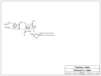
Please see the schematic below. Here the output of opto-coupler is pulsating in nature. If only one sampling is taken for ADC per half cycle of AC then time period for sensing main failure may be as high as 10 ms. If multiple sampling is taken per half cycle and ADC results are averaged then also time factor will be there. Since failure of mains is to be checked constantly, how the result can be achieved. Any tip in this regard will be highly solicited. (I have not utilised this circuit in my inverter design).

regards
swapan


I suppose you need a capacitor at the output of the bridge. to smoothen the wave.
 

I suppose you need a capacitor at the output of the bridge. to smoothen the wave.

In my inverter I have used a small step down transformer for zero crossing detection, mains failure detection and for mains level check as is shown in the schematic below. Everything is ok. But I doubt, as soon as mains fail, the same will be detected a bit later due to the capacitor used for smoothing the signal.

I have come across a inverter circuit that uses a set-up like the other schematic of my earlier post(152). Zero crossing detection is done with the opto-coupler. But no extra circuit is there to detect mains failure. Mains failure as well as mains level is sensed by the said set-up. I have observed the wave form of the signal for ADC using CRO which seems completely pulsating. As there is no separate circuit for mains failure detection, I think it is done by sensing mains level. Either for mains failure or low mains, whenever it goes below a predetermined value, the inverter transfers to inverter mode.

My curiosity is how to utilise ADC so that mains level could be sensed using the earlier schematic.

regards

swapan


Can you explain bit more like what kind of component got damaged of your mobile charger?
Best regards.
M Rahman.

---------- Post added at 23:22 ---------- Previous post was at 22:10 ----------

Dear Swapan,
You correctly saw the pulse which is positive 10ms width and failure of mains is checking continuously not constantly. If you can manage to synchronize inverter’s oscillation with line power frequency then you could able to find pulse duration modulation (PDM). When duration is less than 10ms and average voltage is less than your set value, change the mode. But having said that still I can see other problem according to your schematic, which is how you doing to define line’s positive cycle and inverter’s positive are at the side?
Best regards,
M Rahman
 

Attachments

  • 93_1313480825.png
    93_1313480825.png
    15 KB · Views: 157
Last edited:

I'm working the same project 12VDC 220/240VAC 50Hz inverter with ATMEGA 32. Please send me schematic and Bascom source code to implement yours parts in my projects.
 

Hello there guys,

I have a doubt. This inverter uses what kind of transformer? HF transformer or the 50Hz normal transformer?
 

AoA Tehmid
But tehmid how you are sensing the batter Current and where is the source/Hex Code as this has become a very long awaited Dream Now.
 

what type of shunt r u using and for what purposes chg current only or OL also
 

Status
Not open for further replies.

Similar threads

Part and Inventory Search

Welcome to EDABoard.com

Sponsor

Back
Top