Continue to Site

Welcome to EDAboard.com

Welcome to our site! EDAboard.com is an international Electronics Discussion Forum focused on EDA software, circuits, schematics, books, theory, papers, asic, pld, 8051, DSP, Network, RF, Analog Design, PCB, Service Manuals... and a whole lot more! To participate you need to register. Registration is free. Click here to register now.

analog design solution of pulse creator question

yefj

Advanced Member level 5
Joined
Sep 12, 2019
Messages
1,557
Helped
1
Reputation
2
Reaction score
5
Trophy points
38
Visit site
Activity points
9,376
Hello There is a greate circuit shown below.Is goal is to convert power supply non sinchronios +12V -12V into sinchronios pulse.
It consists of many components which i am having problem to see how they work together.
Why the comparators have capcitor on one leg while the othe leg has resistor?
Why there is a diode after the BJT in the end?
Is there way ou could reccomend me to separate this circuit into parts so i could see the logic ?
LTSPICE file is attached.

Thanks.
1728849140482.png
1728849095904.png
 

Attachments

  • pulse_stabilizer.zip
    2 KB · Views: 44
Still no analog supply or I/O specs? If you convert DC OK to each input then each output is simply a logical sequence state for Off to ON to OFF and risetimes
and delays can be added if necessary and then the input voltage is constantly monitored to be OK at all times.

The solution is much simpler if you learn how to design than trying to teach you how to design.
But if you do not try you won't learn.

It can be old technology analog switches and Flip Flops or a CPLD and window comparators or anything modern with a simple BJT level shifter for the Gate driver but there are no complex analog dependencies, and you can 12V Schmitt logic gates for noise immunity or anything you understand such as Dana's cct.

https://www.ni.com/en/support/docum...emplate-documentation.html#section--631538078 is a starter page on finite state machines. Also look up Karnaugh Map and State Map, the solution is so simple but the foundational logic and language might seem complex.


Now you can get AI to design it for you with the right input (design specs) in a few seconds.

This is what you are lacking all along are complete design specs, not just the FET I/O specs but also all the power up sequence of supplies or fault conditions, thermal sensing, whatever. it must be robust but have tolerances.
 
Last edited:
Hello few questions:
1. if i use opamp with positive feedbak, isnt it going to create stability issues?
2.Why cant we use negative feedback?
3.can i use comperator to do shmidt trigger?
is it better.
 
UPDATE:
Hello FVM.I have implemented shmidt trigger using a comparator.
could you recommend how do i use this shmidt tigger to open my nmos and pmos at the same moment time?
Thanks.
1729185989948.png
 

Attachments

  • smidth_trigger.zip
    7.4 KB · Views: 34
The schmitt trigger is worth pondering as it comes up for consideration. It's a step toward simplifying the design process. (What's needed is simplification.) One or more Schmitt triggers can each be a step in overall startup sequence.

A single assembly can't do everything needed. I think you need several decision-makers. And between them you'll have a place to add another bit of information about the power supply (supplies). Example, zener diode, capacitor time delay.

At some point you want to detect that there's a 23 V difference separating the positive and negative supplies. A 23 V zener can do this.

A fault state from any element halts the start-up sequence.

Searching for further simplification here's the schmitt trigger in IC form. Inverting and non-inverting.

Schmitt trigger icons (buffer n inverting).png
 
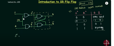
Hello Brad , I looked all over the internet for manuals regarding SR flopflop BJT.
I have here a circuit with "two" switches as shown below.
How can I transform this circuit as Into a circuit that could transform my power supply pulses into fast pulses as shwon below?
How so i need to use SR ?so i could try ans simulate it.
Thanks.

1729454349382.png
1729454011483.png
 
You still have neglected to define the behaviours of your expected performance for thresholds, tolerance (min~max), and Cload etc.
When will you learn to design from specs ?

FWIW

Analog comparators define the thresholds to compare and can have any logic level output.
A "window comparator uses two open collector or drain comparators to define for examples ;​
1. output low if input > upper limit OR < lower limit ..... or​
2. output high if input > lower limit AND < upper limit


Try This

  1. Start power.
  2. Wait for OK logic level on all supplies. Decide on a common interval time for your sequence steps.
  3. Start> Generate a Johnson Counter sequence then stop clock when Tx is ON.
  4. Use up to half the 10 steps for start sequence the rest may be used for Stop sequence..
  5. Assign each output a task with 1st being an All OFF State , others to Set (SR FF) and
    • create any level shift with adequate impedance.
    • Document the specs for each in your Design Spec.
  6. If a fault occurs decide the best response for each.
    • List all the faults you want to cover.
    • Include MUST haves & nice to haves like overtemp, overcurrent or whatever you think is adequate for a robust RADAR system. If something fails how will you diagnose it without sensors?
  7. Stop> enable Clk and the Johnson Counter sequence then stop clock at end and reset.
~ fini ~

  • Outputs may be diode OR logic or using Std Logic or CPLD or uC or SOM.
  • The trick is not to choose yet but to decide how it could function 1st then design it.
  • Not draw something you saw on the internet then ask how do I make it work?
  • Figure out why and how it works first. Update as necessary Design Specs.
  • You will have general design specs like maximum semi, junction temp, maximum resistor junction temp, voltage tolerance target and fail levels, then you will have module specific design specs on how it works and what measurements for I/O.
 
Last edited:
Hello Brad , I looked all over the internet for manuals regarding SR flopflop BJT.
I have here a circuit with "two" switches as shown below.
How can I transform this circuit as Into a circuit that could transform my power supply pulses into fast pulses as shwon below?
How so i need to use SR ?so i could try ans simulate it.
Thanks.
I believe I ought to point back at an earlier schematic you posted. It contains the SR flip-flop... configured and placed in the position to do a particular task in your startup sequence. I'm not saying you ought to use that schematic which someone gave you. My memory is losing track of when you want each Volt level to do something.

I do notice that our angle of approach should be different. I'd rather see each task done step-by-step. The startup sequence consists of decisions interspersed with actions. In other words, mostly logic. Like a chain of logic gates. (I saw a reply mention a state machine.)

Finally if no fault then outcome is to turn on the positive and negative supply transistors.

We (you) still have the shutdown sequence ahead to design yet.
 
Hello Brad, You gave me the schematics of SR flip flop with the two switches.
I have tried to build and simulate as shown below.
But there is this switches issue you shown in the schematcs bellow.
how can i represent these switches in my simulation?
1729507033496.png


1729506899944.png
 
how can i represent these switches in my simulation?
I trust you'll revise your biasing to turn your schematic into an SR flip-flop. You have to end up with a memory cell.

To trigger a change of state electronically requires applying a voltage somewhere. Probably through a resistor. Maybe high, maybe low. There are multiple arrangements of transistors possible. Certain efforts to trigger a change of state are 'forbidden'. Certain efforts are ignored.
 
Hello Brad, So we can look at the situation as logical 1 is +12V and logical zero is -12V.
I dont know why S-R fits this.
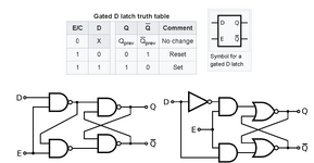
As i see it a D flip flop fits more for the dask.
my data is +12V pulse and clock will be -12V.
So if the clock is low(-12V) the D-flip flop passes the data from input to output.
I think the state which points to the red arrow is the best.
In the web site below i have found a schematics shown below.
In this article logical 0 is 0V and logical 1 is 5V.
So i want to test the d-flip flop truth table:
CLK -5V and data 5V so V_base<V_emiter and Q3 is closed
How can i know what is Q1 base voltag in such situation?
Thanks.

1729584886787.png
1729586367870.png
 

Attachments

  • 1729583936663.png
    1729583936663.png
    205.9 KB · Views: 41
  • 1729584770145.png
    1729584770145.png
    62.3 KB · Views: 42
Hello,I have built a basic simulation in which its working fine. for 0 logic is 0V and 1 is 5V.
I want to transform it to be logical 0 -12V logical 1 +12V.
My +12V and -12V are not idial but they take time to settle as shown in the end.
I want to tranform these not good slow +12V -12V into sharp two pulses of +12V -12V.

I have switched +5V into 12V and GND into -12V.
How can know the formulas for the logical low and logical high threshholds of the advanced circuit so i could tune the circuit?
Thanks.
BASIC simulation:
1729624990725.png

1729625066381.png

Advanced simulation:
1729625106908.png

1729625164487.png
 
I tried to implement it as shown below and in theattached LTSPICE file but the transient transitions translates to the output and the BJT is not opening.
Is there a way to improve the situation?
Thanks.
1729633322250.png

1729633356509.png
 

Attachments

  • advanced_idial2.zip
    863 bytes · Views: 33
Yes a simple Johnson Counter is a 10-stage ring counter (10 cascaded D FFs) which can be modified for any cycle count < 10 or cascaded >10, such as this start-stop sequence and/or reset to initial state (Q1). The app. specs depend on gating the clock with inputs like start/stop and outputs to create a simple state machine with exclusive outputs =1.
--- Updated ---

I tried to implement it as shown below and in theattached LTSPICE file but the transient transitions translates to the output and the BJT is not opening.
Is there a way to improve the situation?
Thanks.
View attachment 194803
View attachment 194804
Why do you have 10s rise time and no high gain comparators? No design specs lead to 1 year of chaotic design. This design is not OK.
Learn to define your basic design specs and how transistors work with simulators until you know it well on static impedance and ratios for each port in CB, CC, CE. (common configs)
 
Last edited:
I tried to implement it as shown below and in theattached LTSPICE file but the transient transitions translates to the output and the BJT is not opening.
Is there a way to improve the situation?
Thanks.
All volt levels need to be adjusted according to resistor values. Likewise all thresholds of operation (changes of state between hi and lo). I don't think your combination of SR flip-flop and D flip-flop is getting you anywhere closer to the startup sequence. (The flip-flops made from NAND gates are handy building blocks and further aid to learning).

My mind is having trouble wrapping itself around the everything-in-one page schematic concept. The interactions become too numerous and too confined.

The Johnson counter (mentioned by Tony) is the type of counter in the 4017 IC (divide-by-10). It's one of the most popular chips ever. Similar to a shift register made from D flip-flops. I believe this is worth pursuing. It's likely to gel into a more linear sequence of electronic events. It should be easier to grasp.
 
Hello Brad,can i just use the chip below?
the problem is I have only +12V -12V , what do i put in VCC?
Thanks.

I have no hands-on experience with it The datasheet makes claims that it monitors your +12 and -12V supplies. Regarding Vcc that's a good question. At first I believed it should run on the same +12 V -12V supply rails as the rest of your circuit.

However I've become puzzled that the schematics don't do that. They give the chip a ground icon yet state it can detect negative voltages. Perhaps it performs some fancy internal level-shifting.

I have a hunch that using the device calls for advanced knowledge from the user. You'll need to decide which is the correct schematic to follow, and which external circuitry to construct, and which values, etc.
Hello Brad ,How do i make it monitor +12V -12V?
How do i connect the chip?
regarding the Vcc i'll try to search more.

1729695127835.png

1729694916505.png
 

LaTeX Commands Quick-Menu:

Similar threads

Part and Inventory Search

Welcome to EDABoard.com

Sponsor

Back
Top