Continue to Site

Welcome to EDAboard.com

Welcome to our site! EDAboard.com is an international Electronics Discussion Forum focused on EDA software, circuits, schematics, books, theory, papers, asic, pld, 8051, DSP, Network, RF, Analog Design, PCB, Service Manuals... and a whole lot more! To participate you need to register. Registration is free. Click here to register now.

600/800W 220~230v AC Inverter SMPS from 12v DC

Status
Not open for further replies.
No ! a shifter needed between these sections ! ( between micro and main driver ! ) 5 to the 15 !
Do I need both? If I operate IR2110 with 12 volt?

goldsmith said:
No ! if your topology is push pull the stress across the DS will be 2vm ! 2*325 ! ( at least ) .
I was talking about the max voltage which will be available at the Transformer output. Say, input voltage is 12v, trans ratio is 34; so, output voltage=12*34=408
In this case, duty cycle has to be around 80% to get avg voltage 325v to be used as inverter input.
 

Hi sam
Do I need both? If I operate IR2110 with 12 volt?
As i can remember it's input circuitry is cmos ! so 5 volts can be considered as zero ! not one ! . so both of them are required !
In this case, duty cycle has to be around 80% to get avg voltage 325v to be used as inverter input.
Who told this ? don't forget that the out put filter should be LC filter ( at least 2nd order and butterworth ) so if the load be higher than normalized impedance of that filter , it can increase the voltage nearby some kilo volts ! is that reasonable ? or when you have overload ! it will decrease ! so you will need feed back from 2nd section tot he first section ! hence your out put voltage should be a bit more than that to create ability of voltage compensation ! by fed path !
Good luck
Goldsmith
 

goldsmith said:
No ! if your topology is push pull the stress across the DS will be 2vm ! 2*325 ! ( at least ) .
My topology is Bridge. Could you please tell a little more on DS and 2Vm? After filtering the converter output, the voltage will be 325v.

Hi sam

As i can remember it's input circuitry is cmos ! so 5 volts can be considered as zero ! not one ! . so both of them are required !
Okay, understood

goldsmith said:
Who told this ? don't forget that the out put filter should be LC filter ( at least 2nd order and butterworth ) so if the load be higher than normalized impedance of that filter , it can increase the voltage nearby some kilo volts ! is that reasonable ? or when you have overload ! it will decrease ! so you will need feed back from 2nd section tot he first section ! hence your out put voltage should be a bit more than that to create ability of voltage compensation ! by fed path !
Yet to design filter as you suggested to make converter part first. For feedback design, I've considered that there is a inverter and the output of the inverter is sine wave. As the inverter terminal voltage is needed to make nearly constant at any load condition, feedback has been taken from there. Here I'm attaching the block diagram of the total inverter system (12v DC to 230v AC). Please check and suggest if there is any mistake.

- - - Updated - - -

12v DC to 230v AC inverter block diagram -
smps-Inverter.jpg

First block "Converter (50kHz)" means the Full Bridge converter at 50kHz operating frequency with a ferrite core transformer. Transformer output waveform is shown in the figure.
 
Last edited:

Hi sam
My topology is Bridge. Could you please tell a little more on DS and 2Vm? After filtering the converter output, the voltage will be 325v.
Take a look at here , please :

And about feedback , i know out put voltage is AC but you should divide it with some resistors ( 2 ) and then rectify and filter it , it will be a variable DC voltage as your feedback for first stage .
Sam , what you are doing ? modified sine wave ? your diagram is for a three level SPWM inverter . i don't think it is necessary to use three level method for this simple aim .
Best Wishes
Goldsmith
 

Hi sam

Take a look at here , please :
Thanks...

And about feedback , i know out put voltage is AC but you should divide it with some resistors ( 2 ) and then rectify and filter it , it will be a variable DC voltage as your feedback for first stage .
Will it be so much variable compare to the voltage at converter output?

Sam , what you are doing ? modified sine wave ? your diagram is for a three level SPWM inverter . i don't think it is necessary to use three level method for this simple aim .
Best Wishes
Goldsmith
This is Modified SPWM https://www.edaboard.com/threads/260091/. Does it seem to be nearer to three level inverter? Dear Goldsmith, generating such waveform should not be complected to me using microcontroller. :smile:
 

Will it be so much variable compare to the voltage at converter output?
Hi sam

No the loop will try to stabilize it !

This is Modified SPWM Modified sinusoidal PWM. Does it seem to be nearer to three level inverter? Dear Goldsmith, generating such waveform should not be complected to me using microcontroller.
I know it is pretty simple to create that waveform . i have designed many inverters based on differentiating SPWM , until now . most important issue will be select a proper stage for power stage . to obtain this waveform . ( you will have at least 4 choice ! ) .
but the only thing that i can't understand here is why you are trying to use a differential SPWM for this simple aim ? because you will need two filter in power stage . and complicated feedback loop ! you have to take a differentiated feedback ! which will be complicated for you , i think ! but if you use a simple link inverter it's THD will be still negligible and of course it's feedback loop won't be complicated ! i couldn't understand what is your application until now . but if you want make that three level , no problem ! you can decrease speed of loop and use that rectifier idea . thus it will be pretty simple .
Good luck
Goldsmith
 

I know it is pretty simple to create that waveform . i have designed many inverters based on differentiating SPWM , until now . most important issue will be select a proper stage for power stage . to obtain this waveform . ( you will have at least 4 choice ! ) .
It would be better if you could please tell a little more...

but the only thing that i can't understand here is why you are trying to use a differential SPWM for this simple aim ? because you will need two filter in power stage . and complicated feedback loop ! you have to take a differentiated feedback ! which will be complicated for you , i think ! but if you use a simple link inverter it's THD will be still negligible and of course it's feedback loop won't be complicated ! i couldn't understand what is your application until now . but if you want make that three level , no problem ! you can decrease speed of loop and use that rectifier idea . thus it will be pretty simple .
Good luck
Goldsmith

My aim is to make a good Inverter practically and learn detail on it as much as possible. After making this I will test with different load conditions. If everything seems okay, I'll use it my house. :smile: But main aim is learning...

I've some queries as below -
(1) Why it will need differentiated feedback and two filters?
(2) Simple link inverter means simple sine PWM? Please suggest the gate waveform that have negligible THD.
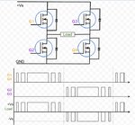
(3) I do not want to make multi level inverter. I wanted to give the SPWM (as per the previously attached figure) gate signal in the MOSFETs connected in H-Bridge configuration.
(4) Could you please tell a little more about "decrease speed of loop"?
 

Hi Sam
It would be better if you could please tell a little more...
Certainly ! you can create two SPWM with messages out of phase together and them get each section to an arm of an H bridge ! and thus the out put wave before filtering will be exactly as you expected !
other way is two different SPWM's ( with a free space ! it will be harder to design and of course it is not an optimum way !
another way is a simple half bridge with minus supply ! which is not good for this aim ! another way is ... ! etc . i think first way would be ok for your aim ( three level SPWM ) .

My aim is to make a good Inverter practically and learn detail on it as much as possible. After making this I will test with different load conditions. If everything seems okay, I'll use it my house. But main aim is learning...
I see , an i know you want learn each thing complete ! it is pretty good and i believe that you will earn success in this process ! ( with hope to the G-O-D )
(1) Why it will need differentiated feedback and two filters?
i told you the best way for feed back in this case is a rectified feed back . and about two filters i think you are referring to the out put power filters before your load ? right ? if yes , each differential SPWM inverter will need two filter to create enough simultaneously thus mathematically both signals will be the same thus subtract of them will be zero but you will have -vsin/2 and + vsin/2 that will consequence , Vsin !
(2) Simple link inverter means simple sine PWM? Please suggest the gate waveform that have negligible THD.
Sam , do you know what is the meaning behind words " high frequency link inverter " ? the process that i have told you for many times called high frequency link inverter ( first section with DC /DC converter and a transformer ( link , here ) and a simple SPWM . it will have low THD too ( you can be sure about lower than 0.1 percent if you correctly and carefully design it ! but as you decided to use a three level SPWM ,
i think it is better that i guide you in your desired path .
(3) I do not want to make multi level inverter. I wanted to give the SPWM (as per the previously attached figure) gate signal in the MOSFETs connected in H-Bridge configuration.
Sam , listen carefully ! the waveform that you need can't be achieved with a simple H bridge ! it will be a bit difference and it is kind of multilevel inverter ! ( three level ) . i told you the simplest way but you told me you want to design it ! and i told you i will help you ! because you are interested in three level method !
4) Could you please tell a little more about "decrease speed of loop"?
Of course ! a rectifier will create a little delay ! and a filter will create another delay too . and this path will affect the first stage it means one stage will have another delay too ! . but in your aim it is not important !
Best Wishes
Goldsmith
 

My topology is Bridge. Could you please tell a little more on DS and 2Vm? After filtering the converter output, the voltage will be 325v.


12v DC to 230v AC inverter block diagram -
View attachment 78448

First block "Converter (50kHz)" means the Full Bridge converter at 50kHz operating frequency with a ferrite core transformer.
Dear sam,
There is is no need to take feed back after the inverter as mentioned in the block diagram you can take a sample from the 325 dc itself, If you keep the 325v dc steady the output voltage of the inverter will be automatically steady since your 325v H bridge is directly driving the load.
regards ani
 

Hi Ani
Dear sam,
There is is no need to take feed back after the inverter as mentioned in the block diagram you can take a sample from the 325 dc itself, If you keep the 325v dc steady the output voltage of the inverter will be automatically steady since your 325v H bridge is directly driving the load.
regards ani
I think you didn't pay attention to things that i have told ! do you know how will be the behavior of a butterworth filter ? and do you know what will happen if the value of load will be higher or lower than normalized impedance of that filter ??! i think you don't know it ! hence you will need a closed loop .
Best Wishes
Goldsmith
 

i told you the best way for feed back in this case is a rectified feed back . and about two filters i think you are referring to the out put power filters before your load ? right ? if yes , each differential SPWM inverter will need two filter to create enough simultaneously thus mathematically both signals will be the same thus subtract of them will be zero but you will have -vsin/2 and + vsin/2 that will consequence , Vsin !
My understanding is - one filter is for 230v, 50Hz output another one is for rectification and filtration of 230v AC to be used as feedback. Am I right now?
Sam , do you know what is the meaning behind words " high frequency link inverter " ? the process that i have told you for many times called high frequency link inverter ( first section with DC /DC converter and a transformer ( link , here ) and a simple SPWM . it will have low THD too ( you can be sure about lower than 0.1 percent if you correctly and carefully design it ! but as you decided to use a three level SPWM ,
i think it is better that i guide you in your desired path .
Yes, understood. I want to make an Inverter with lowest possible THD along with highest possible efficiency. :smile: Please suggest...

Sam , listen carefully ! the waveform that you need can't be achieved with a simple H bridge ! it will be a bit difference and it is kind of multilevel inverter ! ( three level ) . i told you the simplest way but you told me you want to design it ! and i told you i will help you ! because you are interested in three level method !

Three level inverter will require 3 set of H Bridge MOSFET arrangement. Right? Please suggest simplest method to get lowest possible THD and also tell something about 3 level method.

Of course ! a rectifier will create a little delay ! and a filter will create another delay too . and this path will affect the first stage it means one stage will have another delay too ! . but in your aim it is not important !
Understood the delay issue. What is impact of such delay and where it is important?
 

Hi sam
My understanding is - one filter is for 230v, 50Hz output another one is for rectification and filtration of 230v AC to be used as feedback. Am I right now?
You will have two filter for your special H bridge . and then an auxiliary filter ( low power filter ) for feedback path after rectification the fed signal .
And another filter for the first stage . to take average .
Yes, understood. I want to make an Inverter with lowest possible THD along with highest possible efficiency. Please suggest...
thus this method is ok .
Three level inverter will require 3 set of H Bridge MOSFET arrangement. Right? Please suggest simplest method to get lowest possible THD and also tell something about 3 level method.
No ! why you have thought this ? just an H bridge ! but you will have two SPWM . with different messages . and then not of each other ( inverted of each other . ) and then a dead time creation ! and then two mosfet driver . you will have right H side and L side and Left H side and L side . right H side will be SPWM A and right L side will be the inverted signal of SPWMA . and left section : H side SPWMB and L side inverted SPWM B . but don't forget that dead time is most important thing in these inverters .
Sam , may i give you an advice ? if yes , and if it is your first time to design an inverter , i suggest you to start with a usual two level inverter with low power and then you can go through this one ! i have mentioned this because of avoiding from consuming your money and of course your time . in wrong path . then you will have enough experience to do this project . but it is also possible that you be disagree with me .
Understood the delay issue. What is impact of such delay and where it is important?
In AC Current sources with high frequency and in transmitters ! and more other things !
Best Wishes
Goldsmith
 

Hi Ani

I think you didn't pay attention to things that i have told ! do you know how will be the behavior of a butterworth filter ? and do you know what will happen if the value of load will be higher or lower than normalized impedance of that filter ??! i think you don't know it ! hence you will need a closed loop .
Best Wishes
Goldsmith
Hi goldsmith,
I did not mean to say that the feed back is not necessary. The feed back for the smps is a must but what i told is that you can take it(feed back) from 325v Dc sample(after the filter) instead of taking it(feed back) from the output of the 50Hz sine H bridge as shown in sams block diagram in post no 103. is that correct? I am very thankful for the valuable information you are giving on this thread.
regards ani
 
Last edited:

Hi Ani

I did not mean to say that the feed back is not necessary. The feed back for the smps is a must but what i told is that you can take it(feed back) from 325v Dc sample(after the filter) instead of taking it(feed back) from the output of
Let me open the words ! for out put stage you will have a butter worth LC 2nd order filter . to separate message signal from SPWM . this filter will have a normalized impedance . but your load isn't constant . thus it can increase the out put or decrease it . so instability is for this stage not first stage ! but first stage can compensate this problem ! i hope you got the idea .
Best Wishes
Goldsmith
 

Sam , may i give you an advice ? if yes , and if it is your first time to design an inverter , i suggest you to start with a usual two level inverter with low power and then you can go through this one ! i have mentioned this because of avoiding from consuming your money and of course your time . in wrong path . then you will have enough experience to do this project . but it is also possible that you be disagree with me .

Yes, of course. No way to disagree with your proposal. I've no problem going with step by step approach. As I'll make Inverter gate signal using microcontroller, the signal can be changed very easily. It will also help to realize the purity and efficiency of each. But first, need to make converter. Before that the ferrite core transformer. I'll not be able to start practical work before the last week of this month. Before that I'll tr to know more theory in detail from you :smile:


The idea was to make Modified SPWM was as per the attached figure.
Modified-Sinusoidal-PWM-gateSignal.jpg
 
Last edited:

Okay, thanks. I can use MOSFET driver IR2110 to do the same. right?


I want to use microcontroller for both the sections (converter & inverter). Here I was describing the converter section taking feedback from the inverter output. i.e the terminal voltage to be connected to the loads. In this case I considered rms voltage.


Peak voltage will reach 400v and higher. This peak voltage needs to be considered to chose semiconductor devices (e.g, MOSFET). Right?

The peak voltage must be considered. However, where there is ~400VDC, you are using full-bridge and not push-pull. So, choose a MOSFET with a voltage rating above the peak voltage. Make sure you keep some margin for safety.

For driving the MOSFETs from the microcontroller, you can, of course, use IR2110.
 

Hi Tahmid
Are you sure about it ? because it's input gates are Cmos ( as i can remember ) . and a cmos gate won't accept TTL boundaries !

Hi sam
At last i came back again !
Your circuit will give you that waveform as well but it has a big problem . because you shouldn't expect advantages of a differential SPWM from that ! did you understand what i told you about driving the gates for this method really ? and do you know why i have mentioned that way ? do you know what is the big advantage of a three level SPWM method ? i think No .
Best Wishes
Goldsmith
 

Yes I'm sure about that. I've used it before. Searching this forum will give more results of people who've successfully used IR2110 as the driver, with input from microcontroller.

- - - Updated - - -

What needs to be done is to use +5V as the IR2110 "VDD" (pin 9).
 
Hi Tahmid
Thanks for that . i didn't test it with 5 volts and this driver until now . yes you are quite right .
Regards
Goldsmith
 

Status
Not open for further replies.

Similar threads

Part and Inventory Search

Welcome to EDABoard.com

Sponsor

Back
Top