Continue to Site

Welcome to EDAboard.com

Welcome to our site! EDAboard.com is an international Electronics Discussion Forum focused on EDA software, circuits, schematics, books, theory, papers, asic, pld, 8051, DSP, Network, RF, Analog Design, PCB, Service Manuals... and a whole lot more! To participate you need to register. Registration is free. Click here to register now.

multiple bjt switch circuit interpretation

Status
Not open for further replies.

yefj

Advanced Member level 5
Joined
Sep 12, 2019
Messages
1,548
Helped
1
Reputation
2
Reaction score
5
Trophy points
38
Visit site
Activity points
9,328
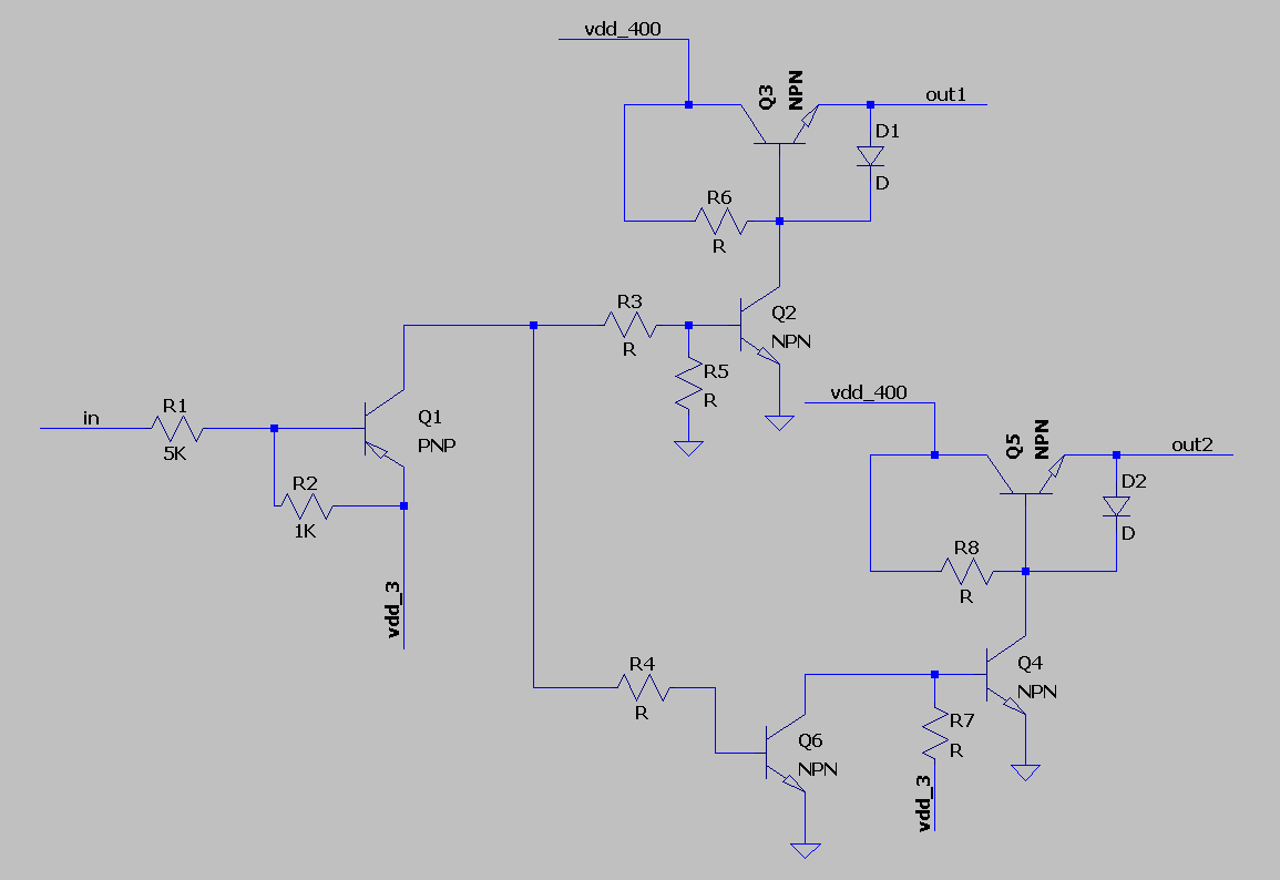
Hello,there is an intresting structure shown bellow, i can that there is a form of switch being used.
from mosfet i know that Vgate above Vt opens the transistor.
But here the bjt's are in weird forms .
how can i interpret the logic of this circuit?
Thanks.

1620677067049.png
 

It seems like you're just trying things at random and
not understanding any of it. Until you either have a
"gut" understanding of how BJTs behave, or can do
the analysis, this will probably not bear fruit.

I much prefer the "gut" approach and it's been fine
across a 30+ year career that's been about 50% bipolar
technology. Though I knew other designers who
much preferred a math approach (like one guy who
really knew his stuff and taught us an internal course
where he derived bipolar operation from the hydrogen
atom and basic physics, over the course of some
months, and was notorious for his 200-transistor
op amp product designs (which met some pretty
good specs, but still)). H-parameters spoke to him.
I just nodded my way through it and kept the notes.

It's often best to work backward from the outcome
desired, through the output drivers and back to the
control-point, establishing robust-to-PVTXYZ "on",
"off" or linear bias for each stage along the way.

You can make use of "switch" primitives and vcvs
sources if you are having trouble with "too many
active devices to understand" and build up from
small sections to larger. Maybe along the way your
gut will get its degree.
 

Hello Audioguru,Yes 2V is fine i just wanted to see the logic of the circuit.
if you be so kind to help me understand the following issues:

1.in the original circuit they have a diode.
Could you please reccomend me a simulation so i could see what its good for?
1621357294399.png


2.
Sorry for viewing things as if its a MOSFET,
On 1 side in the circuit bellow we have current trying to charge bas to Vdd on the other side we have 2 trying to discharge base to ground.
We have a battle between the two.
if we connect R2 instead straight line ,how can we mathematicky portrait this battle?
Thanks.
1621363369931.png
 
Last edited:

The datasheet for every transistor shows a maximum allowed emitter-base voltage of 5V or 6V even if the collector-emitter voltage is hundreds. When the emitter has an inductive load then a very high positive flyback voltage occurs when the transistor turns off that will be much higher than the max allowed voltage and the transistor will be ruined. The diode conducts only when the emitter voltage becomes more positive than the base and limits the flyback voltage to only 0.7V.

There is no battle. Q2 is either turned on and is grounding the base or it is turned off and the base voltage of the output transistor goes as high as it can. Your last schematic shows Q2 turned on all the time with the base and emitter of the output transistor at almost zero volts.
R2 is not needed.
 

Is there a way to simulate this effect?
Thanks.
"The datasheet for every transistor shows a maximum allowed emitter-base voltage of 5V or 6V even if the collector-emitter voltage is hundreds. When the emitter has an inductive load then a very high positive flyback voltage occurs when the transistor turns off that will be much higher than the max allowed voltage and the transistor will be ruined. The diode conducts only when the emitter voltage becomes more positive than the base and limits the flyback voltage to only 0.7V."
 

BJT models generally do not model E-B breakdown
at all (let alone well) and often all you get is a warning
line in the output file, if anyone bothered to set that
up.

The catch-diode ensures that you are not surprised
by the effects of E-B breakdown when the real silicon
hits the real application (at that specific circuit point).
 
Status
Not open for further replies.

Part and Inventory Search

Welcome to EDABoard.com

Sponsor

Back
Top