Continue to Site

Welcome to EDAboard.com

Welcome to our site! EDAboard.com is an international Electronics Discussion Forum focused on EDA software, circuits, schematics, books, theory, papers, asic, pld, 8051, DSP, Network, RF, Analog Design, PCB, Service Manuals... and a whole lot more! To participate you need to register. Registration is free. Click here to register now.

multiple bjt switch circuit interpretation

Status
Not open for further replies.

yefj

Advanced Member level 4
Joined
Sep 12, 2019
Messages
1,395
Helped
1
Reputation
2
Reaction score
5
Trophy points
38
Activity points
8,494
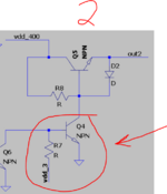
Hello,there is an intresting structure shown bellow, i can that there is a form of switch being used.
from mosfet i know that Vgate above Vt opens the transistor.
But here the bjt's are in weird forms .
how can i interpret the logic of this circuit?
Thanks.


1620677067049.png
 

Hi,

Again my recommendation to do an internet search on your own.

Even wikipedia states "why" it is called emitter follower.

I'm out.

Klaus
 
Last edited:

Yef, you wrongly show a saturated transistor graph when your 2N3906 PNP transistor is not saturated since it has no load and is trying to short-circuit the 3V supply.
The base current needs to be much higher when a transistor is saturated with a very low voltage between collector and emitter.
--- Updated ---

Deja-Vu?
I talked about this odd circuit many times on another website and my sketch over there is in this thread. I never come to this "IC Design" part of this website until now because I buy ICs not design them.
This circuit is not about designing an IC and it is not analog, it is a digital switching circuit and the discussion is about basic transistor operation. Then this thread should be in the Elementary part of this website.
 
Last edited:

How to calcultage the base current in such configuration?(maybe using data sheet of the NPN)
Thanks.

1621228811724.png

--- Updated ---


UPDATE:
I tried to simulate again.I cant see the logic of the currents displayed in the table bellow.
i dont know why base current is so low.
i dont knw how to predict the base current in here

1621230277254.png
 
Last edited:

Hi,

This simulation condition is nonsense.
To see what I mean: disconnect Q1 and see how the currents behave.

Klaus
 

Hello Klauss,thank you for trying to explain me this issue.
I have read the manuals of emmitter follower in AC.
In the DC behavior of a npn in general we need to predict exactly what base current will flow.
I have disconnected the transistor as shown bellow ,We see the currect flow from VDD to Vin1.

What are normal conditions in this situation?So i will see the nonsense in mine.
What is the method to predict the current flow when i put some voltage to the base,in this configuration(with the NPN)

1621238016806.png
 
Last edited:

Hi,

a transitor has no dedicated GND connetion, thus it does not know what "GND" potential is.
Hence it´s not useful to anylyze a bjt behaviour with absolute voltage values (referenced to GND)

A BJT has three terminals: E, B, C
thus you can usefully work with three voltages only:
* V_BE (most meaningful)
* V_CE (almost identically meaningful)
* V_CB (rarely used)

So analyzing your circuit (of post#23) starts with the most important:
--> What is V_BE?
--> and what does this mean for the bjt operation (-point or -state)? OPEN, CLOSED or inbetween?
(refer to my post#14, but mind that you now have an NPN)

Klaus
 

Hello Klauss, I have removed the load and put direct ground to it.
regarding DC region of operation,We have the link to the data sheet of the NPN shown bellow.
Bellow We can see the relevant part of the data sheet .
maximum current accurs at the Saturation state of the BJT when base current cannot be amplifier by HFE anymore.


So Vbe=0.65 Vce=0.2,under those conditions we expect to see I_Base=1mA I_c=10mA
but in reality as you can see in simulation i get base current far less then 1mA.
Where did i go wrong?
Thanks.

1621247659629.png


1621246921656.png
 

Attachments

  • 1621246247151.png
    1621246247151.png
    53.3 KB · Views: 121

I have removed the load and put direct ground to it.
Nobody asked you to do so.

Instead I asked two simple questions...did you answer them?

I really have to stop here, because currently I don´t have the nerve to proceed.

Klaus
 

Yef, why is your simulation applying a very low voltage to the base of the emitter-follower?
When Q4 is turned on then its collector grounds the base of the emitter-follower causing it to be turned off. Then the emitter output is 0V.
When Q4 is turned off the the base resistor of the emitter-follower applies base current which makes the base and emitter voltages rise as high as the base resistor value, beta and load current allow.
 

Hello Audioguru I am just following the datsheet instructions.
I put exactly the VBE and VCE that they said,and i didnt get 1mA current.
 

Hello Audioguru,In the photo bellow I=(5-1)/1K=4mA Vbe=0.63
How do i link R1 to the base current mathematickly?
Thanks.

1621263698113.png
 

You do not feed a voltage to the base of a transistor because it is not a Mosfet. The base-emitter voltage of a transistor is a range of voltages and they change when the temperature changes. The Vbe is from about 0.6V to 0.8V. Since your input to the base is a voltage but not a current then your base resistor R1 does nothing.

The simulation probably uses a "typical" Vbe (around 0.63V) but when you buy transistors you do not know if their Vbe is minimum, typical, maximum or in between.
 

Hello AudioGuru,now i tried to bias it with a current source, i made a 1mA current source in series with 0.65K resistor.
But Vb is 5.66 instead of 0.65V.
Where did i go wrong?
Thanks.

1621267761981.png
 

Hello Audioguru,i did as before,only one resistor.
but I dont know why i get such Vb and Ib,What is the math that gives the simulation those numbers?
Thanks

1621269358689.png

--- Updated ---

UPDATE:
I have found an error,the current source needs to be on the opposite direction.
But againg the problem is i dont know the math of how to control the base current.
i just assume its zero and play with the Ressitor assuming all current goes thre R1 only.
What i nned to do to so i will see 1mA base current?
Thanks.

1621275702184.png
 
Last edited:

I cannot remove the current source because its this stage is following other stages.
Could you give me analisys regarding the the math?

i asked this before also
"What i need to do to so i will see 1mA base current?"
please help me with this part of understanding the math
 

The previous stage is not a current source, it is either saturated at 0V or is nothing (when the previous transistor is turned off it produces no current).
Using the 4.2k ohms then a base current of 1mA is produced when the 4.2k resistor has 4.2V across it which never happens when the emitter load is 1k ohms.

Why do you want the base current to be 1mA? For the emitter output to be +2V at 2mA into the 1k load, the base current must be 2mA/beta. The minimum beta for a 2N3904 is 80 so the base current must be 2mA/80= 25uA. If the emitter is +2V then the base must be +2.7V so the base resistor has (5V - 2.7V=) 2.3V across it and the resistor value is 2.3V/25uA= 92k ohms.

If you want the emitter output to be +4V into 1k ohms then the base voltage will be +4.7V and the base resistor must be 0.3V/40uA= 7.5k ohms.
 

Hello Audioguru,Wow thank you very much.I finaly got the principle as shown in the photo bellow.
but my betha is 300 (this is the Ic/Ib) which is fine as long as the calculations fits the simulation :)
I also succeeded simulating it with the previos stage shown bellow.

In the original circuit our last stage had a diode in it(as shown in the end),its supposed to be something about inductive load ,but i could not understand the logic of inductive load to a diode between collector and base?
Could you please recomend me a simulation to do in order to see why we could use a diode between emitter and gate in the last stage?
Thanks.


1621287089039.png

1621289479609.png
 

Attachments

  • 1621288516675.png
    1621288516675.png
    46.7 KB · Views: 124

I am surprised that your sim program picked a beta as high as 300. Then if you make some of this circuit, a few of them will not work because their beta will be less.
The datasheet of a 2N3904 shows that some have a beta as low as about 80.
Is an output of only 2V at 2mA high enough?
 

Status
Not open for further replies.

Part and Inventory Search

Welcome to EDABoard.com

Sponsor

Back
Top