Continue to Site

Welcome to EDAboard.com

Welcome to our site! EDAboard.com is an international Electronics Discussion Forum focused on EDA software, circuits, schematics, books, theory, papers, asic, pld, 8051, DSP, Network, RF, Analog Design, PCB, Service Manuals... and a whole lot more! To participate you need to register. Registration is free. Click here to register now.

[Moved]: Ultra-low Power Bandgap Reference design

Status
Not open for further replies.
LVT devices will have a larger leakage current due to reduced control of the channel. But since you have a voltage supply of 1V for the amplifier you could probably use standard devices. To get more gain out of the second stage you could self-cascode the output structure. Or you could increase the transconductance of the differential input.

You don't really need to switch to standard VT devices just so you know. Even though the LVTs have more leakage current, just set the quiescent currents in your amplifier to meet your specifications. One thing to keep in mind is that LVTs usually cost extra to fabricate since its not the standard.
 

I need to improve my BGR, it doesn't settle when I vary the supply voltage. Help.

- - - Updated - - -

One thing that you could try that has worked for me in the past is to remove the gate to drain connection of M8. Then connect the output of an op-amp to the gate of M7-M8 and tie the positive node of the op-amp to the drain of M3, the negative node to the gate of M1-M3. If area is not a concern, using a resistor instead of a diode connected MOSFET for M2 might give you better voltage headroom, especially with a supply voltage of 0.45V(is this a superthreshold design or are your devices low VT?). Lastly, the gate of M9 would not be connected to node A, but the gates of M7-M8.

Hi ljp, can you provide me a schematic for this? and do you have any detailed information/guide for this one? Sorry for the demand, I'm just too desperate to work this out.
 

Well first thing, what do you mean it doesn't settle? Is it oscillating? That might be a stability issue with the amplifier then.
 

What I mean is Vref increases upon varying supply voltage.
 

You need to find a way to increase your power supply rejection then. There are a lot of techniques you could use, I'll bet the main reason for the variation is the current variations in your current mirror. You couple other find a structure less sensitive to voltage variations, or make those devices really long (low aspect ratio). Which would increase your overdrive voltage if you're running well into saturation your current will not be changing much provided channel length modulation is minimized(so don't use small devices).
 

aye! Yes, I think the problem is the current mirror. The aspect ratio is just 0.25. Ill make the channel length longer then. Thanks!
 

Yeah try that, let me know if it fixes your problem.
 

Yeah try that, let me know if it fixes your problem.

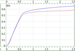
This is the difference between previous work (blue) and updated version (red). It has improved quite well, but the temperature coefficient is about 33ppm/C. I don't know if I should be contented with this so I can move on to LDO.


update.png
 

Looks much better. If 33ppm/C is good enough for your application then that's all you need.

I believe I remember reading that a "good" battery has a TC of 50ppm/C.
 

Looks much better. If 33ppm/C is good enough for your application then that's all you need.

I believe I remember reading that a "good" battery has a TC of 50ppm/C.

I see, thank you. I'll be back again for another update on LDO. :thumbsup:
 

By the way, I'm really curious how robust your design is. If it's not too much of a hassle, would you be able to tell me the variation of your bandgap across Monte Carlo?
 

By the way, I'm really curious how robust your design is. If it's not too much of a hassle, would you be able to tell me the variation of your bandgap across Monte Carlo?

I changed my BGR circuit since my previous design is sensitive to supply variation.

This is the schematic that I'm using now.

Screenshot_1.png

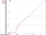
I obtained a reference voltage of 550mV and a regulated output voltage of 1.2V (LDO) from a supply voltage of 1.3V.

Screenshot_3.png
 

Status
Not open for further replies.

Part and Inventory Search

Welcome to EDABoard.com

Sponsor

Back
Top