Continue to Site

Welcome to EDAboard.com

Welcome to our site! EDAboard.com is an international Electronics Discussion Forum focused on EDA software, circuits, schematics, books, theory, papers, asic, pld, 8051, DSP, Network, RF, Analog Design, PCB, Service Manuals... and a whole lot more! To participate you need to register. Registration is free. Click here to register now.

Improving noise question in OPAMP PCB

yefj

Advanced Member level 4
Joined
Sep 12, 2019
Messages
1,237
Helped
1
Reputation
2
Reaction score
3
Trophy points
38
Activity points
7,444
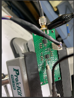
Hello , I have implemented a PCB based on the attached simulation file in the RAR and photo.
I have used ceramic capacitors of 100nF 1uF and 10uF for decoupling.
I tried to put vias on the ground plane to reduce noised.
photos description shown below.
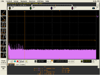
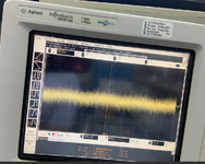
based on the implementation how do you asses the noise level i got ? where could i improve to get a better result then photo 11.PNG zoomed?
Maybe my input signal (11.PNG) is too noisy?
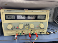
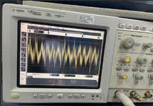
maybe my power supply 7.5V is noisy and the decoupling is not working? (photo 13.PNG)
I only tested the first two stages ,What could be done to improve the result noisewise?
Thanks.

11.PNG is the input signal i get from the signal generator( I tried to simulate both on pure 1mv dc and sine 10mV pk-pk)
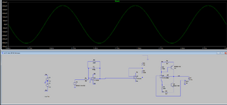
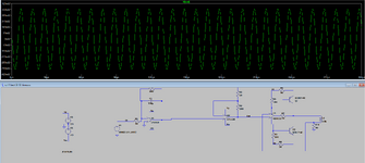
7.png LSPICE simulation
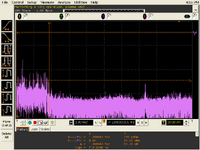
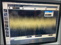
12.png : PCB TEST point of the output
13 .PNG: voltage singal of the input 7.5V from the power supply
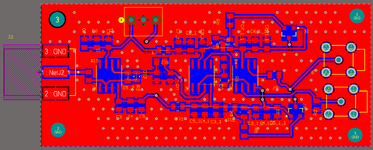
q14.png PCB implementation of the schematics
physical_photos.zip: photos of the ceramic capacitors being used for decoupling.
 

Attachments

  • 8.PNG
    8.PNG
    1.5 MB · Views: 47
  • 7.PNG
    7.PNG
    58.3 KB · Views: 47
  • sch1_LT1028_time.rar
    1.1 KB · Views: 30
  • physical_photos.zip
    7.1 MB · Views: 32
  • q14.PNG
    q14.PNG
    263.7 KB · Views: 51
  • 13.PNG
    13.PNG
    1.8 MB · Views: 46
  • 12.PNG
    12.PNG
    1,002.5 KB · Views: 44
  • 11.PNG
    11.PNG
    1.4 MB · Views: 42
  • 10.PNG
    10.PNG
    1.4 MB · Views: 38
  • 9.PNG
    9.PNG
    1.6 MB · Views: 39
Last edited by a moderator:
Probing considerations, scope probe ground nemesis for getting bad readings :


30 - 40 mV not uncommon. On micro busses I regularly see 200 mV.

OpAmp PSRR degrades substantially at higher freq, consult data sheet for graph.
Ferrite beads + cap to make a LPF can help in some situations.


Capacitor ESR, for same value caps, one vendor to another, and their technology
matter. I did a study of .001, .01 and .1 uF caps years ago, for some RF work, vendor to
vendor huge differences. Qualify your caps with some bench testing.

View attachment 190518


Regards, Dana.
 
Hello Dana,currenly my circuit is purely two opamps.I havent plugged the third stage yet.
I want the output of the second opamp to be the least noisy.
In the ltspice simulation below i put a low pass filter between the opamps which has 1Mhz cutoff frequency,However this filter creates a very high gain peaking which is a sign of oscilations an instability.when i removes the filter i get no gain peaking.
I liked the suggestion to use pherite bead filter.
I can put all kinds filter structures as shown in the laout below.
Is there a pherite bead filter structure i can use similarly to the picture below so it wont get the opamps unstable?
Thanks.
1714742762059.png
1714741334920.png


1714742238693.png


1714742466485.png

--- Updated ---

UPDATE:
can i just put a signle pherite bead between them instead of a filter?
It will act like "RF CHOKE" is it a good idia?
Thanks.

1714743964358.png
 
Last edited:
Hi,

...you think the OPAMP gets unstable.
O.K. ... why not prove it? Just remove the OPAMPs (BTW: you could do the same on your own)
flt1.png

Still "unstable"? even without OPAMP..

And btw: What´s the use of C2?
Just give it a try: let´s remove it:
flt2.png

Nothing changed?

Klaus
 
Ground input to U2 and then look at noise. If its still there guess is its
from power supply, and thats where L >> C >> Vp & same for Vn should
go.

Using FFT on your scope what does noise look like, post a screen shot.


Regards, Dana.
 
Hello Dana, You want me to put ground at the input like shown bellow.what do i need to do with U2?
How should i handle the DC power supply if its the main source of noise?

Hello Klaus,I think its unstable because of there is such a think as gain peaking where we see that the higher the peak the lower phase margin we have :)
You are totaly correct but why am i wrong considering the plot as having gain peaking and potentialy unstable?
Thanks.


1714747552140.png

1714747976009.png
 
Last edited:
The G peaking is not in your fdbk loop, so that does not create "instability",
but can overload a OpAmp G stage with too much input signal. When you do
sims you need to use real models of L and C to get actual peaking values.

You can place the ground at U1 input, take a screen shot of the output, then
ground input U2, screenshot again.

If noise is due to power supply then a LC at each opamp power pin, or try the
main feeds to the board with LC. L in series then C to ground then power pin
or power feed.

1714750023388.png


Regards, Dana.
 
Hi,
Hello Klaus,I think its unstable because of there is such a think as gain peaking where we see that the higher the peak the lower phase margin we have :)
You are totaly correct but why am i wrong considering the plot as having gain peaking and potentialy unstable?
Thanks.

I often have an idea "this is because of ...". Then I prove it, especially when I´m not very experienced in this area. And sometimes I have to see my idea was wrong.

Same is here.
I´ve already proven that the peak (you consider as "unstable") is in first place just the peak of the (unsuitable) filter.

(I mean: you have used L and C only - without any damping resistor. This usually leads to a "resonace catastrophy". My simulation shows a resonance peak of about 50dB. I personally "validate" what this 50dB means. --> This means 1V at the OPAMP output causes more than 300V at the capacitor C3. Again: more than 300V!)

You are free to stay with this "unstability" idea.
My way is a different way. I´d go the next step to prove my idea:
I´d simply replace the LC filter to see what happens. I´d use a filter that does not have this peak ... and see what the stability really is.

The benefit of simulations: ... you can get the result within one minute.
It´s easy and fast to get a clear answer from the simulation. What keeps you from using this benefit? It takes less time than writing a post.
****

Stability of OPAMP circuits:
The stability of an OPAMP circuit mainy is influenced by the feedback loop. But the "filter" you use .. isn´t in the feedback at all.
So for sure it may have a (minor) influence on stability. But it´s not likely to cause an istability with the shown peak.

But I said "mainly". There are other things that influence the stability. Like the load of an OPAMP.
And especially capacitive loads are hard to drive.
This leads back to my question about C2. It´s directly connected to the output of U1!! It´s reactance is 1.6 Ohms at 1MHz .. impossible to drive with an OPAMP!
The OPAMP becomes overloaded and may get hot. Surely operated outside it´s recommended operation conditions.

Usually you don´t want to drive loads larger than some hundreds of picofarads. And since it is a known problem the datasheet shows charts on "capacitve load handling" .. up to huge (for an OPAMP) load capcitance of 10nF. But in your circuit it´s 10x this maximum (of chart) value!

I asked you whats the use of C2? .. no feedback. But it was meant as a serious question.

Klaus
 
Hello Klaus , sorry for the the simple answer.
I went to the internet and used pi filter calculator and picked C L values for a low pass filter with 1MHz cutoff :) that’s why I have two capacitors in the filter.

I want to make a filter with pherite bead as the L( so it won’t store energy) and filter the noise between the first opamp and second opamp.
What values of filter you recommend to use to cut down noise up to 1MHz in my situation.


Or maybe a better Idia is just to put pherite bead between them , to be like RF choke at 1MHz and suppress noise at 1MHz and above , is it a good idia?
Thanks .
 
Last edited:
Always remember the consequence of mismatched impedances at source and load on LC filters.

1. When source of LT1028 @ 1MHz is near 0 ( 150 m0hm with ~16 dB peaking ) at unity active gain
What is the Q voltage gain at breakpoint or resonance? Since it is the noise that is amplified, it will look like a fuzzy sinewave with this Q.

Will adding any series R help to reduce Q ? yes ! = Zo
Have you memorized Q formula yet?

2. When Load of LT1028 is high Z (5pF) ? will loading help? yes but not here , unless you need maximally flat for small signals.

Have you memorized Zo, ωo, equation for a simple 2nd order LC filter yet? Why not?

(Zo~0.75 for L=C1=C2=0.1u) (C1+C2 act in series between source and load.)

Thus all your peaking gain is from mismatched impedances so choose your impedances wisely 1st then low Q or damping factors for desired flatness.

You won't remember if I tell U here. ( Repeat until you can do this with eyes closed)

--- Updated ---

My spec low loss to 1MHz 50 Ohms minimal or no peaking -12 dB/oct

1714774345309.png
 
Last edited:
Hi,
I went to the internet and used pi filter calculator
Why a Pi Filter at all?
I guess you did not investigate what a Pi filter is and waht it is used for.
So I do your job in this regard:
* a Pi filter is a symmetric filter. It works in both directions equally.
* a PI filter often is used in the power supplies, since it helps to reduce Noise in direction power_supply -> external world, but also the other way round, it hepls to reduce external noise to enter the power supply.

You don´t need the "bidirectional feature". No need to use a Pi filter.
Nor do you want to use the filter in a "power supply path".
--> I don´t see why you decided to use a Pi filter at all.
(The same way I don´t see why you are fixed on a ferrite bead now)

More information on "power supply path".
You may want to install a Pi filter in the mains power input of an SMPS. This filter is used to suppess RF noise in both directions. RF noise is in the Megahertz region (stop band) and mains frequency is in the low Hertz (50Hz, 60Hz) region (pass band). RF may be induced in the power cord by a cellular phone nearby( example). You don´t want to enter the cell phone´s noise into the SMPS and possibly manipulation it´s regulation. AND the PI filter is used to suppress the swithing noise of the SMPS to leave the SMPS and cause EMI noise .. and possible affect electronics devices neraby.
--> So stop band is far from pass band. You have an unknown mains side impedance ... and you have a rather unknown (because variable by load, by rectifier..) impedance at the SMPS side. Sine you can not rely on these impedances you need to install the two capacitors to ensure low impedance at high frequencies .. to make the filter reliable work (independent of the used power cord for example)

****
Now you are fixed (no one knows why. There may be a valid reason or not) on ferrite beads.
Your job now: Find out the function and the use cases for ferrite beads.

****
For your application: I can only recommend to NOT look for a solution first.
But first find out / decide the requirements and after that look for a suitable solution.
And this "finding the requirements" starts with defining the "pass band". What frequencies do you need to pass the filter?

****
Example for "finding a solution first":
Let´s imagine your car has a flat tyre.
* YOU go to the garage and buy a new tyre. You come back to the car and see the tyre does not fit the car. You need help in mounting the wrong tyre to your car, with a lot of effort and time consuming.
* OTHER PEOPLE: .. investigate why the tyre is flat. They see that the valve of the tyre is loose. They fix the problem by tighten the valve and pump up the tyre. done. focussed, cheap, fast.

***
You have cosen Pi filter, now you choose ferrite bead.
Why not do an internet search for "low pass filter OPAMP".

Klaus
 
If the noise is broadband, as it appears to be until we get a screenshot of FFT
from a fast scope, or a spectrum analyzer, OpAmps may not be the filter of
choice. Especially as they run out of PSRR and G at noise freq of interest, as OpAmp
GBW is a pproached.

if OP wants to attack it after the fact, in the signal path, one needs more info,
like how far down does he want the noise floor above 1 Mhz.

PI filters in supply paths still a choice of interest, depends as everyone has stated,
on what the source and characteristics of the noise is.

One can certainly filter out noise, and / or attack its generation as solutions to the
problem.


Regards, Dana.
 
Last edited:
Hello Dana , i have soldered the third stage whichin attached schematics as shown below it consists of LT1028 and LT1128.
I have measured the output after R7 at third stage.
Photo 1 output signal with FFT .
Photo 2 only FFT when i input sine wave input
Photo 3 of the board.
Photo 4 is FFT output and analog signl when the input is shorted to gnd.
What is the main source of the noise in your opinion?
How can i try and reduce it?( i have a space for a two directional filter between the first two opmaps)


1715020454757.png

1715020607709.png

1715020791202.png


1715020994077.png
 

Attachments

  • 1715020058477.png
    1715020058477.png
    107.8 KB · Views: 23
Start by measuring your source for SNR, calibrate it. Then measure noise floor of each stage , BW and SNR.

Don't leave a bad photo for us to interpret your settings for noise floor < scan BW (linear/log etc) with useful markers.

There are many reasons for your noise but not enough info to improve it.
 
Hello, Sorry for the low quality photos.I managed to do printscreen of the scope display.

So by the diagram below i described each photo.
What could be the source of the noise and how can i reduce it?(i have space for a pi filter between first and second stages i can use)
Thanks.


1715073605392.png

50 ohm termination on the input and the probe does not touch anything:
50_ohm_term_probe_not touch.png


Input signal with DC connected to the board:

input__with_dc.png


output after first stage when input is ON:


input__with_dc_after_first_stage.png


output after second stage with time domain waveform:

input__with_dc_after_2second_stage.png


output after second stage FFT ONLY:


input__with_dc_after_2second_stage_only_FFT.png


output after 3rd stage FFT only:

input__with_dc_after_3third_stage_only_FFT.png
 

Attachments

  • 50_ohm_term_probe_not touch.png
    50_ohm_term_probe_not touch.png
    50.6 KB · Views: 15
  • input__with_dc_after_3third_stage_only_FFT.png
    input__with_dc_after_3third_stage_only_FFT.png
    59 KB · Views: 13
Thank you for the high quality print screen images.
What is the scale> V/div, dB/div MHz/div?
What are the levels of noise floor, spurious levels in 1st photo, frequency harmonic spacing? Noise source?

The photos should tell a story with all this, but they don't since every FFT data is the same due to your setup error.

Which signals are loaded with 50 ohms? 0dBm = 1 mW or is it dBuv with a 10:1 10M probe? Where is ground reference?

Try to learn how to measure noise with base level dBm or dBuV per Hz of BW and calibrate it with a signal generator so it makes sense to you.

e.g. What is SNR of your signal generator ? What is your DSO noise floor? What is the SNR after each stage of gain? Does it make sense to you? Notice that your SNR reduces with lower frequency due to the CC design with a 1.2uH coil +40 Ohm load. So eliminate the spurious noise in your source then repeat and get the DSO make it easier to compute SNR per root Hz BW

100 kHz signal generator at 1mV, 100 uV, 10 uV so that SNR makes sense to you and the limitations of your DSO FFT then the gain of your amplifiers.

But your 50 Ohm source is not ideal due to some system noise somewhere. (Switching converter EMI ? AM radio signals ?? We call this ingress noise. Radiated is egress.

RF ground is not the same as power ground or signal ground. What is ideal ground? (=0V by definition) What is your ground level?

Cables are less than perfect shields ( semi-rigid coax is much better than braid).
Connectors are not perfect, but SMA should have a torque spec and must never be over-torqued. But this is all low freq. noise so not so sensitive here.

Cable length and routing is important as is DC supply shielding if it has lots of common mode noise and ground is no longer " 0V" or minus infinity in dBuV or dBm. This is how you learn to find your 0V ref in terms of dBm/MHz and make it as low as thermal noise is theoretically possible.

You have measured your 50 ohm signal ground and it is very noisy !

Every component must be considered how it influences the FFT result until it makes sense to you. Changing the FFT filters by sample size and rate will also improve on your use of the FFT

Most of the noise displayed is meaningless DSO so that is your baseline and it can be cut out by raising the display min level so you can focus on your noise source. Then you can identify the fundamental spurious from impulse noise by measuring the spacing of harmonics It looks either like AM radio signals separate by xx kHz or harmonics of SMPS noise coming from somewhere.

Try to help yourself by using the FFT to actually measure noise power in -dBuV/MHz or SNR with a fixed BW in a 50 Ohm conversion for AC coupled 50 ohm terminated DC power then analyze what the LT1080 specs mean converting uV/root(Hz) to dB.


Sorry for a poorly written long-winded reply, but we still do not have enough data.

Notice how your FFT markers stays the same. Use them wisely.

1715087540263.png


I suggest you read Henry Ott's book on EMI from Archive.org I had the original book back in the late 70's with my 1st RF noise problems. It will help you a lot too.
 
Last edited:
BTW camera shots are perfect with a cardboard hood over the display to block FL ceiling lights.

We used a black cube hood attached to camera with Polaroids in our day. Even a pc. of cardboard would work for you.


I can't seem to find it yet either. I think their search algorithm is much worse now. AI not withstanding.

He was the greatest communicator of EMI theory & solutions.


I suspect in 2023 named Henry Ott in the company, after his death in the "Henry Ott Associates", wisely removed all the many published copies since 1958. They are now removed to encourage sales of the most recent publication. Only his publication in 1975 is there, with just the table of contents. https://archive.org/details/noisereductionte0000otth/page/n327/mode/2up


You can only borrow this encyclopedia for one hr.
--- Updated ---

The title of the book has also changed over the decades.
1715091345559.png

--- Updated ---

This book review has brought me fond memories of the wisdom of the version by Henry W. Ott in 1975 when I graduated.


Abdul hanan
5.0 out of 5 stars Easy and to-the-point knowledge
Reviewed in the United States on February 14, 2024
Verified Purchase
Very good book for learning basics of EMC. A chapter about EMC standards is also very good addition.
It has no line written uselessly or overly-explained. I started highlighting the important lines and ended up highlighting every line.
--- Updated ---

Others have tried to copy his work and may be ok, but that's up to you to decide. Ott was the best.

You can get AD's whole book on design for sensors, here is one chapter on GROUNDING.

--- Updated ---

Paul Rako , the Technical Editor For EDN magazine in this article summarizes Henry Ott's advice on isolating noise.

<snip><paste>
1715095202171.png


Is ground logic "0", 0.000 V, Protective Earth, -100 dBm or just a reference for "0 volts" +/- your tolerance or baseline of FFT noise of thermal noise.
( It all depends on your specs)

To summarize my past advice on this CC coil driver design as follows;

1) Locate the circuit it right next to the coil to eliminate C load and coupling noise into a high impedance current source.
2) Use an Op Amp that can drive 50 mA or more without adding noisy BJT common emitter amplifiers unlike common collector.
3) Define your specs before you choose any part.
 
Last edited:
I see that the main noise goes til 1.3MHz. Which is what it was designed for because my amplifier needs to be with 1MHZ bandwidth.
However i am paying the price with amplifying the noise.
Maybe you can reccomend me a filter(i have footprint for pi filter which is free now) i can put between them so it will clean the noise ? given the opamps?
i know i need the filter to be like 10K cutoff but then i need to use very high capacitors which will be between the first and second stages of the opamps and KLAUS already said that they will burn because LT1028 is not built to have 1uF at the load.what could be done?
THanks.
 
Last edited:

LaTeX Commands Quick-Menu:

Similar threads

Part and Inventory Search

Welcome to EDABoard.com

Sponsor

Back
Top