Continue to Site

Welcome to EDAboard.com

Welcome to our site! EDAboard.com is an international Electronics Discussion Forum focused on EDA software, circuits, schematics, books, theory, papers, asic, pld, 8051, DSP, Network, RF, Analog Design, PCB, Service Manuals... and a whole lot more! To participate you need to register. Registration is free. Click here to register now.

I'm tired of hearing noise!

Status
Not open for further replies.
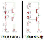
The output above half supply seems to be lower than below half supply. Are both channels showing the same distortion? You have the output transistor connected differently from one channel to the other.

I just noticed that. That is an error in the schematic, but not on the finished board. Both channels are showing the same distortion. If I scope the point before the output capacitor, the sine wave is clearly centered around 4.5V. The op-amp clearly has some issue when sinking current, but not when sourcing it I think :(

The original Cmoy headphones amp used newer and better opamps and used an 18V supply with a Mickey Mouse virtual ground circuit.
Why are you using older opamps and only ONE 9V battery?

What is a "bias capacitor"?

Maybe one or both of your 9V batteries is/are dead.

Please post your detailed schematic.

It has been pointed out several times that NE5532 is a bad idea for a cmoy amplifier (I don't know why though). I looked at some forum where someone had tested a NE5532 so I bought one and tested for myself and was quite happy with it. I then bought 100pcs of them. This was a little over a year a go, I wouldn't have done the same today.

I'm using only one 9V battery to save space. There is no way a simple op-amp can output +-8V or so into 30-60Ohms anyway so I don't see the point of having a supply that huge (other than to avoid some distortions perhaps).

I was talking about the voltage divider capacitor for the non-inverting input (to avoid power supply ripple from entering the amplifier)

The battery is not dead :)

I posted a schematic above, what details are missing? https://obrazki.elektroda.pl/9993570300_1378587719.jpg

edit: I did some further scoping. The distortion is present regardless of frequency and output voltage levels. This makes me think that it has something to do with the output current of the op-amp, but the distortion is gone if I disconnect the headset and only leave the 1k Ohm output cap charge resistors as loads :S Replacing the bjt's with fet's made no difference.
 
Last edited:

There are a number of things you have to consider but before elaborating, desite having such an enthusiastic following, there is nothing clever or particularly good in the design of Cmoy's amplifier. In fact they suffer exactly the same problems as you see now. It's just a design that Cmoy publshed which for some reason attracted lots of followers, most of whom I suspect have never heard a really good amplifier to compare against.

Assuming your schematic has the output transistor emitter pins to the center rail, keeping it in class AB mode will be difficult. AB is probably the best mode to use because it gives a good compromise between power efficiency and good low level distortion. What you have to look at is how to keep both transistors just slightly conducting, in other words with a voltage between base and emitter of about 0.65V. Don't worry about the exact voltage but just consider it has to be there. To turn the top transistor on, the op-amp output voltage has to be more than 0.65V above center rail and to turn the bottom transistor on, it has to be more than 0.65V below it. Clearly it can't be both at the same time so you are using diodes to lift and lower the op-amp output in the direction it's needed. So the diodes alone are resposible for setting the bias point, if 2 x diode Vf isn't the same as 2 x Vbe, the transistors are not optimally biased. This is why an earlier post suggested you thermally bond the diodes to the transistors, as they are both silicon PN junctions, they should be held at the same temperature to improve the bias stability. What you ideally want to do is set the class A to class B change-over point to whatever voltage it needs to make the transistors conduct say 10mA without having to rely on diode matching.

The NE5532, although quite an old device is still regarded as an extremely good audio amplifier - but as a pre-amp, not a power amp. Your purchase was a good one, it's just that you are not using them to best advantage. Note that the data sheet shows optimal performance from a +/- 15V supply and not driving less than 600 Ohms load.

Regarding the output voltage vs. supply voltage: the maximum output you can theoretically get is (the op-amp maximum output) - (2 x Vbe of the output transistors) - (voltage dropped in the emitter resistors) - (voltage dropped in the output coupling components). The data sheet gives 12V output swing into > 600 Ohm load from a 15V supply so a guess would be it can't go closer to supply rails than 2V so your maximum output would be 9V - 4V at the output pin and say 1.5V less than that after the transistors so it probably can't produce more than 3.5V at your headphones. It will distort some way below that. Looking at your oscilloscope trace you are managing very close to that already!

You really need to get rid of that feedback loop from the output back to the NE5532 and keep it local to the preamp stage. The output should have it's own DC stabilization to maintain half rail and a method of controlling the quiescent current to 'just' overcome cross-over distortion. If you can do that, all you will need are some small T0-92 output transistors and they will run almost cold while giving you tons of undistorted volume in the headphones - and no noise!

Brian.
 

The biasing isn't that much of an issue right now, even though I see that I could make some changes. You are right to say that I wan't the bias to be set exactly at the point of conducting to keep the current draw of the amplifier to a minimum. I've made a class B amp in the past with no biasing at all, the cross-over distortion was audible, but it was not like the amplifier was useless. As long as I get 'some' biasing just to get the worst of the cross-over distortion, I will be happy :)

I'm not quite sure why you want local feedback? Having global feedback will make the op-amp adjust for any nonlinearities, try and compensate for any cross-over distortion as well as lower the output impedance (I kind of want an output resistor to avoid having the transistor catch on fire in case of a short).

If I keep turning the volume up, I will get the clipping you are talking about, but this was actually pretty close to the rails. I made this design with the help from this thread, the one with very old high current output transistors and powered from a transformer, this amplifier do not show distortion like this. Regardless, even though the distortion is almost gone at very low output voltage levels (100mVpp or so), it's still there so I don't think this has to do with the output voltage capabilities of the op-amp.

Further scoping shows that the bias point is indeed 4.5V and the output is not shifting from this during load. The output of the amplifier is also producing this distortion so I don't think the output caps are the cause. The input is a smooth sine wave so it's not the input caps either. One odd thing I've encountered a couple of times is that the output looks fine for a couple of seconds after turning the amplifier on, but I find this hard to reproduce, maybe I so desperately want to see a perfect sine wave that I'm imagining things :(

Here's a picture of the output at a lower voltage level, the load is a 33Ohm resistor. You can see that the output goes from -360mV to +250mV so it can sink the current just fine, but not source it?

https://obrazki.elektroda.pl/7238333100_1378633310.jpg
 

Adding feedback over several stages, especially with a phase shift caused by the output capacitor and inductance of the load can cause other problems. What I'm suggesting is you use the NE5532 to best advantage where low noise is needed and use a separately biased output stage, or at least one with a more suitable op-amp in the output stage.

If you really want to stay on this track, try connecting the audio input to the non-inverting pins on the NE5532 and dropping the values of R7/R8 considerably to help it stabilize the DC better. This will also remove the phase shifting effect of the input RC network from the feedback path. Also if possible, use a triangle wave signal source rather then a sine wave, it will show the non-linearity and any cross-over distortion far better than a sine wave can.

Here's an experiment for you to try. Connect the signal generator to one side of your headphone through a 33 Ohm resistor and connect the oscilloscope across the headphone. Sweep your signal generator from say 50Hz through to 20KHz and see if the amplitude varies with frequency. You can also do this by connecting the X input of the scope to the signal generator output and showing an X-Y display. I think you might find the results interesting! If you use the XY method you should see a straight but angled line which stays the same length and angle as you seep the frequency. Try it with the headphones lying open and again with them on a simulated head, anything that seals the cups like a head would will do but I advise against wearing them for reasons of sanity! It will give you some idea of what the amplifier feedback path is trying to compensate for.

Brian.
 

You have a huge error on the output of one channel of the amplifier. Maybe it causes your distortion problem:
 

Attachments

  • amplifier output.png
    amplifier output.png
    15.4 KB · Views: 81

I went back to the original cmoy design (or closer to it at least) with a virtual ground and all, this finally worked! I'm not satisfied until I figure out what the original problem was though :( I will still do the experiment if you think it's still relevant?

R2=10k. C2=470nF, pot=50k.
https://tangentsoft.net/audio/cmoy-tutorial/misc/cmoy-tangent-sch.pdf
 

If you look at your design and the CMoy design you will see some significant differences:

1. CMoy uses 18V supply, you use 9V.
2. CMoy uses the non-inverting input for the signal and the inverting input for the feedback, you use inverting for both.
3. CMoy doesn't use an output coupling capacitor, you do.

CMoy is still prone to instability when driving reactive loads. The output resistor helps to a point but low values provide poor load isolation and high values provide more phase shift in the feedback, both are undesirable.
I can't understand what R1+ and R1- do in the CMoy design. To my mind it would be better to remove them both and connect the center of the batteries to ground instead. You could argue they track center voltage better if one battery voltage was lower than the other but then you could equally argue that differences in capacitances of C1+ and C1- could destroy the LED when you switch off.

You don't have to do my experiment, it was just to demonstrate the effect of putting a reactive load on your amplifier instead of resistive one. I suspect your 32 Ohms headphone varies wildly in impedance across the audio range and seeing what loading effect it had would help to explain why I would keep it out of the feedback path.

Brian.
 

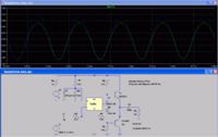
Apparently my explanation how a missing bypass capcitor may cause distortions wasn't well understood, so please review the below simulation.

Battery internal resistance and respective supply drop is the key.


Attachments

  • headphone-amp.zip
    2.2 KB · Views: 52
If you look at your design and the CMoy design you will see some significant differences:

1. CMoy uses 18V supply, you use 9V.
2. CMoy uses the non-inverting input for the signal and the inverting input for the feedback, you use inverting for both.
3. CMoy doesn't use an output coupling capacitor, you do.

CMoy is still prone to instability when driving reactive loads. The output resistor helps to a point but low values provide poor load isolation and high values provide more phase shift in the feedback, both are undesirable.
I can't understand what R1+ and R1- do in the CMoy design. To my mind it would be better to remove them both and connect the center of the batteries to ground instead. You could argue they track center voltage better if one battery voltage was lower than the other but then you could equally argue that differences in capacitances of C1+ and C1- could destroy the LED when you switch off.

You don't have to do my experiment, it was just to demonstrate the effect of putting a reactive load on your amplifier instead of resistive one. I suspect your 32 Ohms headphone varies wildly in impedance across the audio range and seeing what loading effect it had would help to explain why I would keep it out of the feedback path.

Brian.

Yes, i know they are different, but I use a virtual ground and no output coupling cap in the latest design I just made (the one that worked), only difference being the supply voltage. I would like to put this design (the one with no output stage and output decoupling cap) to rest and rather just make amplifiers with a class AB output stage, the output power is so much better as well. In order to do this though, I have to fix the distortion issue I have with the single rail design :( Another option would be to use a virtual ground, but I have had issues with this voltage divider virtual ground before (that's why I like the single rail design so much better).

Apparently my explanation how a missing bypass capcitor may cause distortions wasn't well understood, so please review the below simulation.

Battery internal resistance and respective supply drop is the key.

I don't have LTspice installed, so I can't view the simulation. I assume that it's not a coincidence that the distortion you show is exactly what I am having trouble with! What are the difference between the blue and green graph though? With and without the bypass capacitor? I did actually start to think of battery voltage drop and how that could be the cause of the distortion, but I only measured like 20-30mOhm between the supply pins and the battery connector. The one thing that has been the common factor with all these designs is the battery! I've run out of 9V batteries, so I just stole the battery from my Uni-T DMM. The battery gets a ripple of 300mV during heavy load! I will add a bypass capacitor to see the difference. Thanks a lot FvM! :D

Edit: I added 1uF capacitors and it worked like a charm (I can't fit anything bigger without making a new board). I'm so glad I finally fixed it :D
 
Last edited:

LTSpice is free, so you can check the simulation with acceptable effort if you are interested. The 10 ohm series resistance in my simulation is modelling the battery internal impedance. The value sounds reasonable for a small 9V block.

The specific problem of this circuit is that the supply voltage only drops during positive halfwaves when the upper output transistor sources current, so a half-wave rectified voltage is feed through the bias network and superimposed to the signal voltage.
 
Yeah, I understand the theory behind it. It might be easier to just add a big current reservoir cap to the supply rather than having bypass capacitor by the feedback path, no? I have honestly never thought of the battery impedance playing a role in distortion's, but it's not hard to see how :p
 

I just started thinking of that bypass capacitor and how big this have to be. In an inverting design that I've been making, any ripple in the supply caused by current draw from the amplifier will lead to distortion, but how much distortion? If I know the supply ripple, how do I then find the minimum capacitor value needed so that the distortion isn't audible?

Adding feedback over several stages, especially with a phase shift caused by the output capacitor and inductance of the load can cause other problems. What I'm suggesting is you use the NE5532 to best advantage where low noise is needed and use a separately biased output stage, or at least one with a more suitable op-amp in the output stage.

What other issues can global feedback cause? I would like to know the pro's and con's between global and local feedback in a design like this. I'm picturing the op-amp as a wonder maker, compensating for everything (as long as it doesn't oscillate that is). The op-amp will do everything it can to keep the output of the output stage at the same level as Vin*gain, what will prevent it from doing so? Also, if I'm going with local feedback and low output impedance, how do I short circuit protect it?
 

"I posted a schematic above, what details are missing? http://obrazki.elektroda.pl/9993570300_1378587719.jpg"

For starters, where do the right-side terminals of C3 and C5 connect to??
 

Nothing, as the schematic shows :p R10 and R16 are connected to +V along with the collector of the bjt's, I failed to show that.
 

I would like to reopen the thread, I have an issue with a design I posted earlier in the thread, I'll re-post the schematic:


This problem is a new one, I just can't figure it out. If no load is connected, both channels are working superbly. If a load is connected (testing with 2x 1kOhm at the moment), everything is just fine as long as I'm giving the same sine wave to both inputs. The odd thing is that if I disconnect one input, both output's will start to output only one half of the sine wave :O I've done some scoping and I clearly see a sine wave present at the input of one op-amp, but not the other. The op-amp with no input will still output half of the sine wave even though there's nothing but a little noise present on the non-inverting input. I can't help to feel that this has to do with some heavy cross talk or something, but I'm clueless :O Surprisingly, the amplifier sounds okay, but songs that I know rely heavily on stereo (sounds bouncing from one ear to the other for instance) just sounds like broken mono.
 

The center tap is connected to ground yeah. I figured out that issue, it was so obvious that I'm a little ashamed. I have trouble when connecting 6.35mm jacks for some reason, I didn't connect it all the way in so the contact points were shifted :(
 

Status
Not open for further replies.

Similar threads

Part and Inventory Search

Welcome to EDABoard.com

Sponsor

Back
Top