Continue to Site

Welcome to EDAboard.com

Welcome to our site! EDAboard.com is an international Electronics Discussion Forum focused on EDA software, circuits, schematics, books, theory, papers, asic, pld, 8051, DSP, Network, RF, Analog Design, PCB, Service Manuals... and a whole lot more! To participate you need to register. Registration is free. Click here to register now.

How to interface BP Transducer to PIC18F?

Status
Not open for further replies.
Hi,

I assume there is some misunderstanding at your side.
Can anybody show how to solve these equations to get 0 to 5V DAC voltage = +/-18V to +/-2V Output?
This is impossible in my eyes:

****

The TI document designs a circuit to make an output voltage from -10V ... +10V (output can be positive as well as negative = bipolar) with a DAC output voltage of 0V...2.5V (positive values only = unipolar)
The formula is: V_OUT = 8 x V_DAC - 10V
V_DAC --> V_OUT
0V --> -10V
0.5V --> -6V
1.0V --> -2V
1.5V --> +2V
2.0V --> +6V
2.5V --> +10V

If you want a +/-2V output...
= the output voltage to alternate form -2V to +2V and back --> you need to alternate the DAC_output from 1.0V to 1.5V and back.

Klaus
 
That is what I am doing, I am toggling the DAC output say between 0V and 5V using Tijmer1 and Timer3 interrupts but not getting the required signals. I am simulating in Proteus the stimulator part bu inputting 0 to 5V Pulse instead of DAC output.

I am trying ti.com document and also this.

https://masteringelectronicsdesign.com/differential-amplifier-calculator-2/

but both ar enot working.

For 0V DAC output my Stimulator signal should be +/-2V and for 5V DAC output my stimulator signal should be +/-18V. How to get these signals? Which document should I follow? Above link or ti.com doc?

Can you show the resistor values for ti.com circuit?

If +/-2V to +/-18V circuit is not possible or difficult to design then tell me how to get +/-18V signal from 0 to 5V DAC toggle and +/-9V signal from 0 to 2.5V DAC toggle.


I need like this.

V_DAC --> V_OUT
0V --> -2V
0.1V --> +2V


V_DAC --> V_OUT
0V --> -18V
5V --> +18V

The ti.com circuit never worked for me.

For 0 to 2.5V pulse it gives 0 to 10V signal out.
For 0 to 0.1V it gives 0V to 400mV signal.
The signal never goes negative.

I am not using VREF in circuit because my DAC VREF is 5V and it is internal to PIC.
 

Attachments

  • UP2BP3.png
    UP2BP3.png
    32.9 KB · Views: 85
Last edited:

Hi,

For ideal OPAMPs your circuit of post#18 should work.
for "ideal"!

But your OPAMP is not ideal, thus I posted in post#19:
Note: this is against Common mode input voltage specification of your OPAMP, because IN+ = 18V but it´s specified to be +Supply -2V which is 18V-2V = 16V

You simply are beyond specification!

*****
And also pleas note that going to the rails is not what an OPAMP is meant to do. Always leave some headroom. Even rail to rail ones need some 10s of millivolt of headroom.
Otherwise the OPAMP may go into saturation and may not behave as you expect.

*****
To your requirement:
0V --> -18V (or close to it)
2.5V --> +18V (or close to it)

input range is 2.5V -0V = 2.5V
ouput range is +18V -(-18V) = 36V

Gain = ouput range / input range = 2.5V / 36V = 14.4
Offset (ouput referred) = -18V

Thus the overall formlua shuld be: V_out = V_in * 14.4 -18V

*****

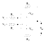
To simplfy things I use the "difference OPAMP circuit" or "differential amplifier circuit".
diffamp.gif
* V2 is the positive input
* V1 is the input reference
* OPAMP output = output
* right of bottom R2 = output reference

Connect V2 to your DAC
Since you want to reference the input to GND --> connect V1 to GND
Connect the OPAMP output to your "stimulator"
Since you want to reference the output to -18V --> connect the right of R2 to -18V

Gain = R2/R1.
Let´s make R1 = 10k then R2 = 14.4 * 10k = 144k

finished.

Klaus
 
Still not working for me.

Maybe there is some misunderstanding.

When DAC output toggles between 0 and 5V the OPAMP otput should toggle between -18V to +18V.
When DAC output toggles between 0 and 2.5V the OPAMP otput should toggle between -9V to +9V.
When DAC output toggles between 0 and 0.1V the OPAMP otput should toggle between -0.72V to +0.72V.

Vout/Vin = 36/5 = 7.2.

0.1V * 7.2 = 0.72V
 

Attachments

  • U2B1a.png
    U2B1a.png
    22.2 KB · Views: 88
  • U2B1b.png
    U2B1b.png
    19.5 KB · Views: 100
  • U2B.rar
    15.2 KB · Views: 99
Last edited:

Hi,

You are still wrong.

When DAC output toggles between 0 and 5V the OPAMP otput should toggle between -18V to +18V.
When DAC output toggles between 0 and 2.5V the OPAMP otput should toggle between -9V to +9V.
When DAC output toggles between 0 and 0.1V the OPAMP otput should toggle between -0.72V to +0.72V.

Correct is:
(Please use the formula from post#23:)
Thus the overall formula shuld be: V_out = V_in * 14.4 -18V

* 0V will give -18V
* 5V will give +18V

But if you want -9V and +9V, then you obviously can't use 0V, because this gives -18V.
Again the formula: V_out = V_in * 14.4 -18V
You want V_out to be -9V...
The formula now is: -9V = V_in * 14.4 -18V
Now solve it for V_in ... and get 0.625V
--> You need a DAC voltage of 0.625 to get -9V at the output.

Klaus
 
Finally, I got success with the circuit.

Here it is.

In actual circuit, RV1 will be replaced with another 10-bit internal DAC (DAC2) output. And when DAC1 is toggling between (0 and 5V) the DAC2 will give fixed 5V (same as high level of DAC1) and this will get converted to -18.0V from U2.

If DAC1 toggles between 0 and 2.5V then DAC2 outputs fixed 2.5V and U2 output -9.0V. So, we get final output as +/-9.0V.

Thank you Klaus for the circuit and equations.
 

Attachments

  • U2B4a.png
    U2B4a.png
    31.8 KB · Views: 98
Last edited:

Please tell me how to get SBP and DBP readings from the sensor using ADC input. I am not using any filters either hardware or software. There is one Microchip application note with c source code for BP monitor using pIC24.

https://www.microchip.com/wwwAppNotes/AppNotes.aspx?appnote=en565742

I am using only one channel ADC to read the sensor which gives 0 to 2.5V for 0 to 250 mmHg. For stimulator part I need to read 0 to 60 mmHg but totally I have to read 0 to 250 mmHg.
Can I implement PIC24's c code into PIC16F by porting it? If yes, what changes needs to be done?
I need to get SBP and DBP readings and from them get MAP (Mean Arterial Pressure) readings and then calculate 5% steps of MAP to control stimulator signal amplitude and pattern.
 

Hi,
You are still wrong.
Klaus

Getting the correct voltage now. Did the +/-2V offset in DAC code.

Any changes needed for Stimulator part? How to limit Stimulator current? I am using 24-0-24V 2A transformer. I guess 100mA is the max current that can be applied to the subject. So, should I use a series resistor at the OAPMP output to limit the current?
 

Attachments

  • SS1.png
    SS1.png
    153.1 KB · Views: 101
  • SS2.png
    SS2.png
    152.9 KB · Views: 111

I am referring AN1556 and trying to copy most of the BPM, filter, math code to my mikroC PRO PIC project. The required files like math.h, math.c, filter.h, filter.c, waveform_tables.h, waveform_tables.c got ported directly without need of any changes.

https://www.microchip.com/wwwAppNotes/AppNotes.aspx?appnote=en565742

I just want to know what changes I have to make to my hardware (ADC input side, like Internal OPAMP based filter, I have one Internal OPAMP free to use). How to port the PIC24F circuits filter circuits at ADC input to my circuit?
In coding part, how should I read ADC?, Should I use two channels similar to PIC24F's code and take 250 samples for each channel (2 channels) alternately (can't do simultaneous readings of 2 channels in PIC16F) using TimerX Interrupt?

Should I use ADC Interrupt and Timer Interrupt to take the readings and then process it after each 500 (250 x 2) samples are taken?

I just need to get SBP (Systolic Blood Pressure) and DBP (Diastolic Blood Pressure) readings to find out MAP (Mean Arterial Pressure) value from an equation and calculate 5% of current MAP value and control the Stimulator signal amplitude between +/-2V to +/-18V for 60 mmHg to 0 mmHg BP.

1 sec = 1000 ms

1000 ms / 500 (samples) = 2 ms

So, should I read one channel for 2 ms and another channel for 2ms alternately for 1 sec to get 250 samples per channel and use it to find SBP and DBP?
 

Please refer page 6 of

https://ww1.microchip.com/downloads/en/AppNotes/00001556B.pdf

and answer.

LPF Fc0 = 1/(2P*R16*C14) = 1/(2P*10000*1u) = 15.92Hz
C12 and R15 = HPF

C15 and C13 are for what and what values I can use for them?
What is DC_OFFSET and why it is needed?
Can DC_OFFEST be GND?

Fc1 = 1/(2p*R15*C12) = 0.48 Hz
Fc2 = 1/(2p*R25*C21) = 4.8 Hz

I will retain LPF (R16, C14) and HPF (0.33uF, R15)
I will alo retain R25 and C21 but change R24

How to find out R24?
I know that it is just an non-inverting amplifier and

Vout/Vin = (1 + Rf/Ri)

My Vout should be 5V
Ri = (R25) = 1k

How can I know what will be the max voltage at OPA2P2 pin?
My sensor output max voltage is 2.5V for 250 mmHg BP and it is fed at R16 input.
I am not usingh INA.

If I know the voltage max at OPA2P2 pin which will be my Vin then I can calculate Rf (R24).
 

Hi,

I didn't go through the complete AN .... just the schematic.

C15, C13 = dnp = do not populate (I assume)

Offset:
The output of a HPF is bipolar (positive as well as negative), but your ADC can manage positive signal only. Thus a DC voltage (offset) is added, higher than the most negative output of the HPF .... to ensure the result is positive only.
The problem is the same as your previous "unipolar to bipolar conversion", but the other way round.
Once you understand the one, you will understand the other, too.
The most useful value for the offset voltage is: (ADC_input_volt_max - ADC_input_volt_min) / 2

Can DC offset be GND?
Yes, but only if you use an ADC which can handle negative input voltages.

How to find out R24?
With the given formula "gain2= ..." (next to R24 in the schematic)

How can I know what will be the max voltage at OPA2P2 pin?
You talk as if it is a DC voltage...like 2.3V,
But it is AC, thus you always have to calculate with the minimum expectable voltage and the maximum expectable voltage in your waveform (both peak voltages).
The magnitude of the AC voltage depends on the expectable pressure (min, max peak) and the gain of your circuit.

Klaus
 
Please refer BP sensor datasheet in post #1.

The sensor that now we are using gives only 0 to 2.5V max = 0 to 250 mmHg BP. So, the output of HPF will not be negative, right? Then I can use GND as DC_OFFSET?
My sensor signal is similar to a Half Wave Rectifier output that is we are using a Syringe instead of a pump to take the measurement and when the syringe is pushed the reading goes max 2.5V. If the syringe is not pushed it is 0V.


Edit:

By referring this

https://www.electronics-tutorials.ws/filter/filter_3.html

and using DC_OFFSET = GND

if my sensor output is 0 to 2.5V then output of HPF is unipolar and 70.7% sensor voltage = 2.5V * 0.707 = 1.7675 and I have to get 5V from this to feed ADC.
So,

5/1.7675 = (1 + Rf/1000)
Rf = 1.8k

Is, this correct?
 
Last edited:

Hi,

The sensor that now we are using gives only 0 to 2.5V max = 0 to 250 mmHg BP. So, the output of HPF will not be negative, right? Then I can use GND as DC_OFFSET?
I recommed to learn basics of hardware...

It still is like already written.
"The output of a HPF is bipolar (positive as well as negative), but your ADC can manage positive signal only. Thus a DC voltage (offset) is added, higher than the most negative output of the HPF .... to ensure the result is positive only."
"The most useful value for the offset voltage is: (ADC_input_volt_max - ADC_input_volt_min) / 2"

My sensor signal is similar to a Half Wave Rectifier output that is we are using a Syringe instead of a pump to take the measurement and when the syringe is pushed the reading goes max 2.5V. If the syringe is not pushed it is 0V.
I don´t understand this completely. But for the problem it is meaningless.

Klaus
 

Syringe is used as a pump and when it is not pushed the sensor reading is 0V and when it is pushed to max the sensor output goes 2.5V max.
 

Not getting 5V output at OPAMP output when the input to the circuit is 2.5V.
 

Attachments

  • SS3.png
    SS3.png
    25.9 KB · Views: 81

Hi,

Makes no sense. The OPAMP output can´t be 5V DC.

Klaus

P.S.
Maybe it helps you to understand the signal if you simulate with an meaningful heartbeat signal.
 

I have new issue. I am not getting 20 Hz signal with this code but getting 5 Hz signal. What is the issue?

32 MHz Clock, Fosc/4 = 8 MHz. 8 MHz INTOSC + x4 PLL.

F = 20 Hz
T = 1/20 = 50ms
Ton = 25ms
Toff = 25ms

50ms * 20 = 1 sec

Timer Prescalar is 1:4
Timer reload value = 15536

1/(Fosc/4/4/65536) = 1/(32000000/4/4/65536) = 32.768ms

1/(Fosc/4/4) = 1/(32000000/4/4) = 0.5us

Required timer1 interrupt is 25 ms

25ms/0.5us = 50000

65536 - 50000 = 15536


Code C - [expand]
1
2
3
4
5
6
7
8
9
10
11
12
13
14
15
16
17
18
19
20
21
22
23
24
25
26
27
28
29
30
31
32
33
34
35
36
37
38
39
40
41
42
43
44
45
46
47
48
49
50
51
52
53
54
55
56
57
58
59
60
61
62
63
64
65
66
67
68
69
70
71
72
73
74
75
76
77
78
79
80
81
82
83
84
85
86
87
88
89
90
91
92
93
94
95
96
97
98
99
100
101
102
103
104
105
106
107
108
109
110
111
112
113
114
115
116
117
118
119
120
121
122
123
124
125
126
127
128
129
130
131
132
133
134
135
136
137
138
139
140
141
142
143
144
145
146
147
148
149
150
151
152
153
154
155
156
157
158
159
160
161
162
163
164
165
166
167
168
169
170
171
172
173
174
175
176
177
#define _XTAL_FREQ 32000000UL
 
 
// PIC16F1779 Configuration Bit Settings
 
// 'C' source line config statements
 
// CONFIG1
#pragma config FOSC = INTOSC    // Oscillator Selection Bits (INTOSC oscillator: I/O function on CLKIN pin)
#pragma config WDTE = OFF       // Watchdog Timer Enable (WDT disabled)
#pragma config PWRTE = ON       // Power-up Timer Enable (PWRT enabled)
#pragma config MCLRE = ON       // MCLR Pin Function Select (MCLR/VPP pin function is MCLR)
#pragma config CP = OFF         // Flash Program Memory Code Protection (Program memory code protection is disabled)
#pragma config BOREN = ON       // Brown-out Reset Enable (Brown-out Reset enabled)
#pragma config CLKOUTEN = OFF   // Clock Out Enable (CLKOUT function is disabled. I/O or oscillator function on the CLKOUT pin)
#pragma config IESO = ON        // Internal/External Switchover Mode (Internal/External Switchover Mode is enabled)
#pragma config FCMEN = ON       // Fail-Safe Clock Monitor Enable (Fail-Safe Clock Monitor is enabled)
 
// CONFIG2
#pragma config WRT = OFF        // Flash Memory Self-Write Protection (Write protection off)
#pragma config PPS1WAY = ON     // Peripheral Pin Select one-way control (The PPSLOCK bit cannot be cleared once it is set by software)
#pragma config ZCD = OFF        // Zero-cross detect disable (Zero-cross detect circuit is disabled at POR)
#pragma config PLLEN = ON       // Phase Lock Loop enable (4x PLL is always enabled)
#pragma config STVREN = ON      // Stack Overflow/Underflow Reset Enable (Stack Overflow or Underflow will cause a Reset)
#pragma config BORV = LO        // Brown-out Reset Voltage Selection (Brown-out Reset Voltage (Vbor), low trip point selected.)
#pragma config LPBOR = OFF      // Low-Power Brown Out Reset (Low-Power BOR is disabled)
#pragma config LVP = OFF        // Low-Voltage Programming Enable (High-voltage on MCLR/VPP must be used for programming)
 
// #pragma config statements should precede project file includes.
// Use project enums instead of #define for ON and OFF.
 
#include <xc.h>
#include <stdio.h>
#include <stdlib.h>
 
unsigned int timer1ReloadValue = 15536;
unsigned int dacValue = 1023;
char toggleDacOutput = 0;
 
//Timer1
//Prescaler 1:4; TMR1 Preload = 15536; Actual Interrupt Time : 25 ms
void InitTimer1() {
    T1CON = 0x21;
    PIR1bits.TMR1IF = 0;
    TMR1H = 0x3C;
    TMR1L = 0xB0;
    timer1ReloadValue = 15536;
    PIE1bits.TMR1IE = 1;
}
 
void __interrupt () my_isr_routine (void) {                                  
    if((PIE1bits.TMR1IE) && (PIR1bits.TMR1IF)) {
        PIR1bits.TMR1IF = 0;
        TMR1H = timer1ReloadValue >> 8;
        TMR1L = timer1ReloadValue;
 
        toggleDacOutput = ~toggleDacOutput;
 
        if(toggleDacOutput) {
            DAC1REFH = dacValue >> 8;
            DAC1REFL = dacValue;
            DAC6REFH = dacValue >> 8;
            DAC6REFL = dacValue;
        }
        else {
            DAC1REFH = 0;
            DAC1REFL = 0;
        }
 
        DACLDbits.DAC6LD = 1;
        DACLDbits.DAC1LD = 1;
    }
}            
 
void initailizePorts() {
    TRISA = 0x33;
    TRISB = 0x08;
    TRISC = 0x21;
    TRISD = 0x00;
    TRISE = 0x00;
 
    PORTA = 0x00;
    PORTB = 0x00;
    PORTC = 0x00;
    PORTD = 0x00;
    PORTE = 0x00;
 
    LATA = 0x00;
    LATB = 0x00;
    LATC = 0x00;
    LATD = 0x00;
    LATE = 0x00;
 
    ODCONA = 0x00;
    ODCONB = 0x00;
    ODCONC = 0x00;
    ODCOND = 0x00;
    ODCONE = 0x00;
 
    WPUA = 0x00;
    WPUB = 0x00;
    WPUC = 0x00;
    WPUD = 0x00;
    WPUE = 0x00;
 
    HIDRVB = 0x00;
 
    SLRCONA = 0x00;
    SLRCONB = 0x00;
    SLRCONC = 0x00;
    SLRCOND = 0x00;
    SLRCONE = 0x00;
}
 
void initailizeADC() {
    ANSELA = 0x37;
    ANSELB = 0x0A;
    ANSELC = 0x60;
    ANSELD = 0x00;
    ANSELE = 0x02;
 
    ADCON0 = 0x00;
    ADCON1 = 0b11100000;
    ADCON2 = 0x00;
}
 
void initailizeDAC() {
    FVRCON = 0x00;
    DAC1CON0 = 0xA0;
    DAC1REFH = 0x00;
    DAC1REFL = 0x00;
    DAC1CON0bits.DACOE1 = 1;
    DACLDbits.DAC1LD = 1;
 
    DAC6CON0 = 0xA0;
    DAC6REFH = 0x00;
    DAC6REFL = 0x00;
    DACLDbits.DAC6LD = 1;
    
}
 
void initailizeOPAMP() {
    OPA1CON = 0x80;
    OPA1ORS = 0x00;
    OPA1NCHS = 0x00;
    OPA1PCHS = 0x00;
 
    OPA2CON = 0x90;
    OPA2ORS = 0x00;
    OPA2NCHS = 0x00;
    OPA2PCHS = 0x00;
 
    OPA3CON = 0x90;
    OPA3ORS = 0x00;
    OPA3NCHS = 0x00;
    OPA3PCHS = 0x00;
}
 
int main(int argc, char** argv) {
    OSCCON = 0xF3;
    OSCSTAT = 0x51;
    OSCTUNE = 0x00;
 
    initailizePorts();
    initailizeDAC();
    initailizeOPAMP();
    
    DAC1REFH = dacValue >> 8;
    DAC1REFL = dacValue;
    InitTimer1();
    INTCONbits.PEIE = 1;
    INTCONbits.GIE = 1;
    
    while(1);
    
    return (EXIT_SUCCESS);
}


Edit:

Issue solved.

I had to set SCS bits of OSCCON to 00.
 
Last edited:

I got stimulator (DAC signals shown in image) signals fine but want to know if I have to use the Active filter circuit at ADC input side. See attached images which shows the actual BP sensor output voltage.

Stimulator signals also fine for 0 to 60 mmHG BP.

Just want to know if I need a filter at ADC input to get the readings of SBP and DBP as done in AN1556?

I don't have the actual sensor to test and so Client is testing the ADC working at his site. I am only testing ADC working with a POT.

So, What signal I can use for BP sensor output to test the ADC working at my site?

Find the attached current circuit as PDF.

- - - Updated - - -

Edit:

5V = 1023 raw DAC value = 0 mmHg BP
0.56V = 0144 raw DAC value = 60 mmHg BP

1023 = 5V
0114 = y

y = (114 * 5) / 1023 = 0.56V

You can see that 0.56V is giving +/-2V Stimulator signal in Proteus simulation screenshot.
For 5V DAC (Buffered with OPA3OUT) we are getting +/-18V Stimulator signal as tested on hardware and also in Proteus Simulation.

- - - Updated - - -

Who can help me with reading the BP sensor?

I got stimulator signals fine as tested on my hardware. DAc voltage varies as needed and also turn Off if BP is greater than 60 mmHg + Hysteresis = 246 raw ADC value + Hysteresis.

Video file is big ad my youtube upload reduced the video resolution and hence I am posting like to video if someone wants to see.

https://mega.nz/#!KFQGAA7b!tAqyLT-6LwFU7vimW2vFLzI0egwUSxXULW43MQEPdBw

For now, it is just Logic Analyzer capture of buffered DAC outputs.
 

Attachments

  • WhatsApp Image 2019-05-31 at 2.48.47 AM.jpeg
    WhatsApp Image 2019-05-31 at 2.48.47 AM.jpeg
    96.1 KB · Views: 78
  • WhatsApp Image 2019-05-31 at 2.54.15 AM.jpeg
    WhatsApp Image 2019-05-31 at 2.54.15 AM.jpeg
    144.6 KB · Views: 88
  • LA4-1.png
    LA4-1.png
    55.2 KB · Views: 88
  • STIMULATOR-1.jpg
    STIMULATOR-1.jpg
    534 KB · Views: 100
  • LA3.png
    LA3.png
    42 KB · Views: 81
  • BPM+STIMU.PDF
    52.5 KB · Views: 107
Last edited:

I am referring this.

https://www.microchip.com/wwwAppNotes/AppNotes.aspx?appnote=en565742

Please check ADC ISR code in it and also the AN1556 PDF.

Why they have used hardware filter?
Why there are reading ADC1 and ADC2 channels?
What do ADC1 and ADC2 readings give?

If I use PIC16F without simultaneous ADC sampling how can I read ADC 1 and ADC two channels when similar ADC interface circuit as in AN1556 is used?
 

I studied An1556 and understood the working of the device. It seems it is not possible to implement BPM using PIC16F which cannot do simultaneous ADC samplings. I decided to use PIC24FJ128GC101 same as AN1556 device for the project. I will also retain the An1556's filter and DAC circuits. I will use the same code as An1556 but ported to mikroC PRO dsPIC (already ported).

My BP sensor gives 0 to 250 mmHg = 0 to 2.5V DC.

So, should I use the INA used in AN1556? Or can I directly feed my sensor output to filter?

I will be using 3 external Microchip 12-bit DAcs to get the stimulator output signal and also the sensor signal on DAC for analysis.
 

Status
Not open for further replies.

Similar threads

Part and Inventory Search

Welcome to EDABoard.com

Sponsor

Back
Top