Continue to Site

Welcome to EDAboard.com

Welcome to our site! EDAboard.com is an international Electronics Discussion Forum focused on EDA software, circuits, schematics, books, theory, papers, asic, pld, 8051, DSP, Network, RF, Analog Design, PCB, Service Manuals... and a whole lot more! To participate you need to register. Registration is free. Click here to register now.

Fluctuating voltage from a bad transistor

Status
Not open for further replies.
Nobody can determine from the schematic snippets if the said transistor actually needs protection, in other words if the driving signal can exceed Vbe,max. But the clamping action will be as described.
 

In the circuit under discussion, you have to check what's "behind" CR20. Discharging the capacitor C19 through CR20 is the only way to drive CR19 into forward bias (clamping action).
 

Using Transistors as switches

Don't they have hysteresis problems? how do you not have hysteresis when using transistors as a switch?
 

Using Transistors as switches

Don't they have hysteresis problems? how do you not have hysteresis when using transistors as a switch?
Normally a transistor switch has no hysteresis. It simply switches on or switches off.
You can add hysteresis to a transistor switch if you want.

Hysteresis is simply some positive feedback.

- - - Updated - - -

Normally a transistor switch has no hysteresis. Hysteresis can be added if you want.
 

Normally a transistor switch has no hysteresis. It simply switches on or switches off.
You can add hysteresis to a transistor switch if you want.

When do you need to add hysteresis to a transistor switch? when the input on the base is what kind of signal?

Why would a designer add hysteresis to a transistor switch? for what reason?

Hysteresis is simply some positive feedback

Why would positive feedback give you hysteresis?
 

89517d1365918131-npn-pic-1.jpg

Transistor Q2 work as switch, circuit is time-delay. When power is on, C19 charged through R52 to 12V and approximately 15000*0.00022=3s Q2 is on, after this time Q2 is off. When on anode CR20 comes ground, C19 discharged through CR20 and CR19. On base Q2 is negative voltage, drop limited by CR19 to -0.7V , Q2 is off. When on anode CR20 comes positive voltage, C19 charged again through R52 to 12V and 3s Q2 is on, after this time Q2 is off.
 

470 uF capacitor? It is probably an electrolytic type. Have you checked to see if it has dried out and is now an open circuit????
 

Thank you pplus for info.

Do yo know what these transistors are doing and are they switches and what kind?

IMG_20130422_171706_624.jpgIMG_20130422_171711_373.jpgIMG_20130422_171717_322.jpgIMG_20130422_171720_662.jpg

- - - Updated - - -

I'm confused on how the transistors switch works

How does the transistor switch turn on? its from the collector

Mostly I have seen transistor switch turn on from the base
 

Yes they are operated as switches meaning the Vce is saturated.

Unlike linear mode, current gain is irrelevant in spec given for non-saturated condition.

It is most often specified to force design to use current gains of 10 when in saturated mode,. THis means you calculate base current then collector can be up to 10x base current at rated saturated voltage. This is intended for low impedance signals or power switch drivers. So it can be slow On/off or fast data.

So 10K to 15V means 15-0.7V = 14.3V/10K = 1.43 mA base current so recommended load is ~15 mA for Vce= < 0.5V But more current only raises Vce voltage
 

I'm confused on how the transistors switch works

How does the transistor switch turn on? its from the collector

Mostly I have seen transistor switch turn on from the base
Will you be posting arbitrary schematic snippets in this thread for the next weeks? How they are related to the thread title?
 

Thank you pplus for info.


I'm confused on how the transistors switch works

How does the transistor switch turn on? its from the collector

Mostly I have seen transistor switch turn on from the base

5407644800_1366698577.jpg


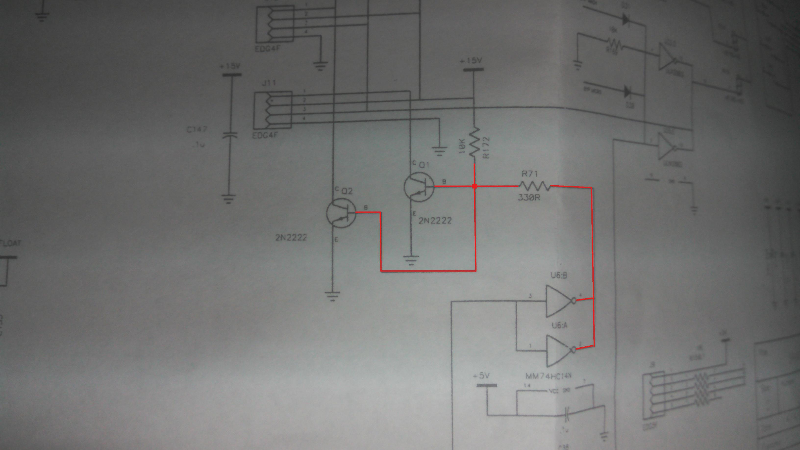
It is usual switch, controlled by U6.

PS The quality of your documentation surprised me. Points in junctions are not put specially?
 

What is this transistor doing? is it a switch? or controlling the current?

Transistor#1.jpg

- - - Updated - - -

This is a Transistor Switch with DC offset from the diodes right? how does it work tho?

NPN pic#2.jpg

How does it turn on and off, I think when the transistor is ON it has DC offset, when the transistor is OFF there is No DC offset, Is there any hysteresis?
 

I agree, the question is poorly worded, the schematic is poorly done and the design purpose is secret.

This is a standard BAD practice of trying to increase the drive current of a CMOS using NPN using parallel inverter and parallel transistor. We call this a buffered level shifter as the output pullup can be any voltage. ( which is not shown) Using a base resistor 10K to 15V adds some drive but not much.

It shows that the designer does not know how to design drivers even if it works.. sort of.

I drew it quickly from left to right as this is the standard practice from input to output, to see if you recognize the design yet.
buf.gif

This question needs more clarity. ( understatement)
 
Last edited:

My manager said that
FETS are for switching Low Current, low voltage
Transistors are for switching High current, High voltage

FETS have high impedance

FETS need to be discharged , because the gate has capacitance that needs to be discharged

Transistors collect to emitter has a Resistance that causes a voltage drop , where a FETS source to drain doesn't have a voltage drop or resistance

- - - Updated - - -

Why would you want to do Level shifting/shifter? for what reason?
 

NPN pic#2.jpg

I'm not sure why the transistor switch doesn't go to Zero voltage because of the 2 diodes on the emitter

Any reason why the designer didn't want the Turn OFF position of the transistor to not go to zero voltage but to 1.4 volts?

What reasons would it be for a transistor switch's OFF state to be at 1.4 volts instead of zero volts?
 

What is this transistor doing? is it a switch? or controlling the current?
89905d1365908735-transistor-1.jpg

Since U114 is a comparator with hysteresis, it is logical to assume that the Q119 is a switch that transmits the reference voltage of the comparator to an other part of the scheme.

- - - Updated - - -

View attachment 89946

I'm not sure why the transistor switch doesn't go to Zero voltage because of the 2 diodes on the emitter

Any reason why the designer didn't want the Turn OFF position of the transistor to not go to zero voltage but to 1.4 volts?

What reasons would it be for a transistor switch's OFF state to be at 1.4 volts instead of zero volts?
Here I can not say anything. I do not see where does the input signal, where does the voltage at R2A and R2A own nominal value, and which comes output Q1A and Q2A.

PS I strongly recommend reading
The Art of Electronics
Student Manual for the Art of Electronics
 
Last edited:

Status
Not open for further replies.

Part and Inventory Search

Welcome to EDABoard.com

Sponsor

Back
Top