fixing design for simultanios excitation of a sequencer
- Thread starter yefj
- Start date

D.A.(Tony)Stewart
Advanced Member level 7

- Joined
- Sep 26, 2007
- Messages
- 10,298
- Helped
- 1,868
- Reputation
- 3,741
- Reaction score
- 2,518
- Trophy points
- 1,413
- Location
- Richmond Hill, ON, Canada
- Activity points
- 64,908
The criteria for the supply filter is the attenuation greater than 6.02 dB or phase shift in the signal BW.
I assume a matched load to source impedance = 6.02 dB.
Modify my assumptions to your design.
Parasitic inductance should be included with an estimate of ESL=0.5~0.6 (?) [nH/mm] for short traces and ln(l/w) ratio.
I assume a matched load to source impedance = 6.02 dB.
Modify my assumptions to your design.
Parasitic inductance should be included with an estimate of ESL=0.5~0.6 (?) [nH/mm] for short traces and ln(l/w) ratio.
yefj
Advanced Member level 5

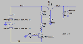
Hello, So basickly its a filter to pass the pulse to the amplifier
In Ltspice I have made equivalent circuit with AC transfer function response with 5Mhz BW 69Mhz.
the original circuit acts good but as you can see in the last photo When i lowered the 1.1uH to 100nH an the pulse goes threw much better.
One dilemma I have regarding the load.I will connect this circuit to spectrum analyzer.
What load do i need to put in the simulation to test the response?
Thanks.
https://www.rfwireless-world.com/calculators/Rise-Time-to-Bandwidth-Calculator.html
Attachments
D.A.(Tony)Stewart
Advanced Member level 7
- Joined
- Sep 26, 2007
- Messages
- 10,298
- Helped
- 1,868
- Reputation
- 3,741
- Reaction score
- 2,518
- Trophy points
- 1,413
- Location
- Richmond Hill, ON, Canada
- Activity points
- 64,908
This evaluation filter circuit is a filter design used to block microwave power signals from feeding back into the DC source, from the amplifier RF out connected to an external RF load (e.g. some Radar RF power port.)
The filter uses inductors (L1, L2, L3) are low Z near DC and high Z at RF defined as "parasitic components such as parasitic capacitance (Cp) and DC resistance (DCR).
The Capacitors may be std LF or RF ceramic NP0/C0G types , which have the lowest ESR and ESL parasitics too. But if you are talking about 10GHz+ RF these cannot be ignored.
Any significant change in component values affects the spectral impedance and attenuation in both directions.
These dual direction attenuations may be computed by scattering (s) parameters or S-parms. or s11, s12, s21, s22.
Key points include:
Above all, every Gnd symbol on the schematic must be 0 V +/- ?? tolerance for noise from DC to > 10GHz. This tolerance is defined by the perturbation limits of s-parms and the EMC interference levels of the Device Under Test (DUT) for both emissions and susceptibility. **
Anecdotal
I recall a large 14" disk drive near the top floor of the tallest building in Winnipeg, in the heart of the financial district was getting random soft and hard errors. It was later found to be caused by the 1kHz pulsing of RF from the airport Radar as its antenna was rotating when synchronized with a data read/write in sync along with other events. Improved shielding/grounding of the R/W RF signal path was the fix.
The filter uses inductors (L1, L2, L3) are low Z near DC and high Z at RF defined as "parasitic components such as parasitic capacitance (Cp) and DC resistance (DCR).
The Capacitors may be std LF or RF ceramic NP0/C0G types , which have the lowest ESR and ESL parasitics too. But if you are talking about 10GHz+ RF these cannot be ignored.
Any significant change in component values affects the spectral impedance and attenuation in both directions.
These dual direction attenuations may be computed by scattering (s) parameters or S-parms. or s11, s12, s21, s22.
Key points include:
- The filter allows low-loss DC to pass while blocking RF signals from reflecting into the DC source.
- The design ensures high return loss (high RF signal loss) into the DC source, providing high impedance to RF.
- The filter’s behavior and performance are influenced by parasitics, and design choices must consider impedance effects within the bandwidth of the DC voltage regulator.
Above all, every Gnd symbol on the schematic must be 0 V +/- ?? tolerance for noise from DC to > 10GHz. This tolerance is defined by the perturbation limits of s-parms and the EMC interference levels of the Device Under Test (DUT) for both emissions and susceptibility. **
Anecdotal
I recall a large 14" disk drive near the top floor of the tallest building in Winnipeg, in the heart of the financial district was getting random soft and hard errors. It was later found to be caused by the 1kHz pulsing of RF from the airport Radar as its antenna was rotating when synchronized with a data read/write in sync along with other events. Improved shielding/grounding of the R/W RF signal path was the fix.
yefj
Advanced Member level 5
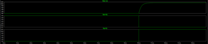
Hello Tony, So one simulation i did is to see how a pulse will pass threw .
did my 50Ohm load is ok? did i do it ok?As you saw in the plot the bandwidth is 60MHz.
Does the filter works both ways? how can i Know the load when the RF signal tried to climb up the DC power source?
Thanks.
did my 50Ohm load is ok? did i do it ok?As you saw in the plot the bandwidth is 60MHz.
Does the filter works both ways? how can i Know the load when the RF signal tried to climb up the DC power source?
Thanks.
D.A.(Tony)Stewart
Advanced Member level 7
- Joined
- Sep 26, 2007
- Messages
- 10,298
- Helped
- 1,868
- Reputation
- 3,741
- Reaction score
- 2,518
- Trophy points
- 1,413
- Location
- Richmond Hill, ON, Canada
- Activity points
- 64,908
no DC source terminal is << 1 OhmHello Tony, So one simulation i did is to see how a pulse will pass threw .
did my 50Ohm load is ok?
no you must examine bandwidth of signal and DC regulator source as expected. RF signal GHz, and DC BW MHzdid i do it ok?As you saw in the plot the bandwidth is 60MHz
As usual Yes.
Does the filter works both ways?
Computing s21, If Vout no load is 12V on Drain and is loaded by RF 50 Ohms at 125 mA then Vo = 50*.125A= 6.25 V and Drain RdsOn will be near 50 Ohms with matched Z then attenuation should be 6 dB ~ and any additional attenuation is due to absorption by the DC line filter. This is slightly impacted by the 301 ohms on R1 by 0.25 dB as I remember and improved by reducing the 301 slightly.how can i Know the load when the RF signal tried to climb up the DC power source?
Thanks.
This design of the demo board is different than previous company owners who used RC filters for every port LF and RF supply & gnd. So any change affects in both directions. I'm not sure of the assumptions for the design but you must simulate with accurate RLC values for every part to realize more accurately.
Similar threads
-
-
-
Design of input capacitors for switched-mode power supplies?
- Started by asrock70
- Replies: 5
-
-