Continue to Site

Welcome to EDAboard.com

Welcome to our site! EDAboard.com is an international Electronics Discussion Forum focused on EDA software, circuits, schematics, books, theory, papers, asic, pld, 8051, DSP, Network, RF, Analog Design, PCB, Service Manuals... and a whole lot more! To participate you need to register. Registration is free. Click here to register now.

fixing design for simultanios excitation of a sequencer

yefj

Advanced Member level 4
Joined
Sep 12, 2019
Messages
1,411
Helped
1
Reputation
2
Reaction score
5
Trophy points
38
Activity points
8,595
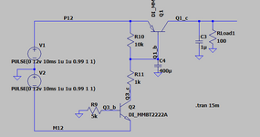
Hello,The circuit is supposed to delay the output of P12 because the PNP is opening gradually.
In previos version it worked great but i put P12 as a pulse and circuit just not working.
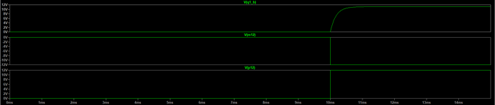
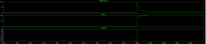
The Veb is totally different.Veb is supposed to be 0 and rise gradually.
But when i made P12 0-12V pulse my Veb is tottaly ruined.
How can i fix it so Veb will rise gradually from 0 till PNP is opening?
LTSPICE file is attached.
Thanks.
 

Attachments

  • 1.PNG
    1.PNG
    10.7 KB · Views: 14
  • 2.PNG
    2.PNG
    12.6 KB · Views: 10
  • 3.PNG
    3.PNG
    11 KB · Views: 11
  • test4.zip
    4.7 KB · Views: 5
Last edited:
Hello Brad, both the power rails are created at the same time.
Its like i connect them to the power supply push the button and +12 and -12 appear as I push the button.
I can change it to what ever you want,
The problem is the my Veb gone very bad.Its supposed to start with zero and gradually rise thus opning the PNP after a while so +12 will be on the output.
How can I fix the situation?
LTspice file is attached.
Thanks.

1726476808626.png
1726476677331.png

--- Updated ---

UPDATE:
Hello,There was a basic flaw in my simulation because Vb started from 12V and went down.
In here our Vb start to zero So Veb is 12V and going down Thus its always open.
Is there a way to fix it?
Thanks.

1726477532510.png
 

Attachments

  • test4.zip
    4.7 KB · Views: 6
Last edited:
1726479207615.png


Curious why you have Q2 terminal labels as Q3_c and Q3_b ?

1726479801609.png


You rapidly turn on Q2 while at the same time supply power to Q1 emitter, but at that point in time
C4 discharged (unless you stipulated its initial condition charged), so R11 supplies much more
current to keep C4 discharged, at close to 0V, hence Q1 conducting than R10 does trying to turn off
Q1 by charging C4.....?
 
"Curious why you have Q2 terminal labels as Q3_c and Q3_b ?"
Yes there is no Q3 , i should label them as Q2.

Yes I understand C4 is discharged and Q1 is always open so no delay and P12 going thew Q1 as the Pulses rises.
How do you recommend to create a delay so Q1 will be closed and after a while it will open thus allowing P12 to pass threw Q1_c?
Thanks.
1726482168345.png
 
What is max rate you will do turn on/off cycles ?

What is max current you will need for load ?

1726487572558.png


Regards, Dana.
 
Last edited:
There is an ~ 5 mS transient due on power up where load does come on, then
as long a power is continuous the transient no longer occurs when supply switched
on and off, pending OP answer to rate of turn on/off subsequent.

Additional transistor can manage that, could hold off load by switching is ground aide
(easy)......or other approaches. Or simple do the switching of the ground lead of load,
get rid of PNP as a pass element.

As always a low end micro, like an ATTINY85 series, could easily manage the sequencing fault
free including debouncing signal to turn on/off.....
 
Last edited:
Hello, When i will build it in my lab and i will turn on the power supply.

capacitor has the tendency to be continues with voltage , so id there is a voltage jump on one side it will transform to the other side .

So the quetion is about the capacitor.

When we send a pulse on P12 How C4 will behave?
Why the Gnd on the other side ruins it?
Thanks.

1726590590697.png
 
When you turn on power C4 charges up thru R10. But note in my sims your R11 is the 11K,
R10 the 1K.

When a cap has no charge on it and a V applied to it it looks like a short, and as charge is acquired
starts to look like an increasing impedance, hence a dropping current thru it.

1726595899426.png
 
Hello Dana,my question is what is the difference between the situation of state 1 of the capacitor when its other side is grounded and the situation 2 when C4 is parralel to R10.
Purely on the point of view of the capacitor how it will handle the pulse in both cases?
Thanks.

1726605191934.png
 
When we send a pulse on P12 How C4 will behave?
Why the Gnd on the other side ruins it?
I see it plain as day. The PNP internal PN junction and bias wire give no opposition to enormous startup surge current. This immediately goes through C4 to ground.

For one solution remove C4. Possibly change the PNP to NPN. More work needs to be done on the delay timing function.
 
Here is working delay, but initial transient artifact :

1726606582717.png


Here is C moved ( I will let you do the sims going forward ) :

1726607336230.png


Looks like initial transient removed.
 
Last edited:
I see it plain as day. The PNP internal PN junction and bias wire give no opposition to enormous startup surge current. This immediately goes through C4 to ground.

For one solution remove C4. Possibly change the PNP to NPN. More work needs to be done on the delay timing function.


Hello Brad,My focus is on the C4 capacitor.I was told that the difference between situation 1 when C4 is grounded the base of Q1 starts from 0V.

When C4 in parralel to R10 then C4 starts from 15V. What is the inner capacitance mechanism that caused the difference?
Thanks.

1726639691770.png
 
In either situation C4 starts at 0V. It has no charge. Q = C x V or V = Q / C, if Q is initially 0
then so is V of capacitor.
Thats why your idea to move C4 across Q1 B-E junction worked, the design is started with Vbe = 0
so Ic = 0.

1726653056606.png
 
Last edited:
Hello Dana, If we look again at sitation 2 when C4 is parralel to R10, I can say than when pulse is coming one side of the capacitor is 12V and the other is zero.
What preventing the capacitor to be 12V as soon as the pulse comes?
Thanks.

1726660155641.png
 
What is the timing relationship you want / will have between P12 pulse and M12 ?

What is delay from M12 to Load power on you want ?

Are you in complete control regarding timing of P12 and M12 ?

This assumes that you power up circuit at P12, that then essentially stays on,
and only when M12 asserted does power come on and stay on for as long as M12 asserted. ?
That M12 from that point on is primary control of power to load ? Unless of course entire
system turned off.

Like this -
1726665589992.png

--- Updated ---

Here is sim file you can experiment with, attached.

Download Simetrix, just google it. There is a free version that is more than
adequate for most simple sims.
 

Attachments

  • Slow Turnon Power.zip
    4.4 KB · Views: 1
Last edited:
Hello Brad,My focus is on the C4 capacitor.I was told that the difference between situation 1 when C4 is grounded the base of Q1 starts from 0V.

When C4 in parralel to R10 then C4 starts from 15V. What is the inner capacitance mechanism that caused the difference?
Previously C4 had no resistance inline. Current was free to travel directly through the PNP and out through its base. Then to C4 which went directly to ground.

Basic rule of PNP operation is that we turn it on by withdrawing current from the base. This current then has a path to ground (or lesser volt level) by going through neighboring components.

So C4 charged immediately turning on the PNP immediately. When C4 was charged, current stopped through C4 and the PNP turned off. This interfered with the timing delay function.
 

Base current bipolar :

1726669812976.png


Primary external influence is Vbe.

Emiiter current bipolar :

1726669899421.png


Again primarily a function of Vbe.

--- Updated ---


What preventing the capacitor to be 12V as soon as the pulse comes?
In this circuit the cap charges thru R11 and Q2 when it is on, cap across R10. Note
if Q2 off there are leakage currents that can charge cap, but much slower as leakage
currents quite small in todays general purpose low power type transistors. Concern would be
if Ileak x R10 >= ~ Vbe, or Ileak =~ Vbe (.7V) / 10K =~ 70 uA. So you want Q2 leakage when
off to be (with 10 x margin) < 7 uA. the 2222 Icbo hot is 10 uA max, so you are probably
OK with R10's value. You can sim leakage behavior in Simetrix quite easily versus Temperature,
predominant cause.

When cap is Q1 base to ground it charges thru R10, independent Q2.

1726670394953.png
 
Last edited:
Hello Brad , So in the original case C4 was directly charged by P12 and it charges very fast.
In the upgraded version there is no pass to the ground from the base .
What what is physically happening to the capacitor
We have a capacitor in parallel to R10, a pulse is coming .
How it will react? It will start charging .
What is the difference of charging in the first and second case?
When pulse comes Veb is not 12 automatically .
why in the second case C4 is charged slower?
Thanks .
 
Last edited:

LaTeX Commands Quick-Menu:

Similar threads

Part and Inventory Search

Welcome to EDABoard.com

Sponsor

Back
Top