Continue to Site

Welcome to EDAboard.com

Welcome to our site! EDAboard.com is an international Electronics Discussion Forum focused on EDA software, circuits, schematics, books, theory, papers, asic, pld, 8051, DSP, Network, RF, Analog Design, PCB, Service Manuals... and a whole lot more! To participate you need to register. Registration is free. Click here to register now.

Fast switching transistor with slow rise/fall times, why?

Status
Not open for further replies.
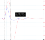
You could tighten-up your layout quite a lot. You don't want to have large diameter current loops if you want clean fast waveforms. You also want to minimize wiring inductances where possible.

- - - Updated - - -

Some more waveforms.
 

Attachments

  • T5.png
    T5.png
    46.1 KB · Views: 104
  • VF1.png
    VF1.png
    60.9 KB · Views: 116

You could tighten-up your layout quite a lot. You don't want to have large diameter current loops if you want clean fast waveforms. You also want to minimize wiring inductances where possible.

- - - Updated - - -

Some more waveforms.
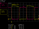
I'll go down to the local brick and mortar shop and scoop up some virgin pcb. I'll let you know when my version 2.0 (Tight Millenium Edition) is ready. Thank you.

- - - Updated - - -

If you add a 1uH inductor in series with the power source in the idealized simulation schematic, almost gives same ringing waveforms... that is why I am asking the above questions.

That was exactly my thought too, but I attributed that to the scope probes and/or the load bulbs.
 

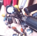
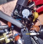
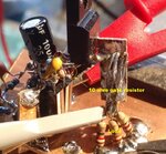
Here are some more close-up shots showing the tight layout on the pcb.
 

Attachments

  • layout_2.jpg
    layout_2.jpg
    445.3 KB · Views: 108
  • layout_1.jpg
    layout_1.jpg
    72 KB · Views: 98
  • Like
Reactions: CataM

    CataM

    Points: 2
    Helpful Answer Positive Rating
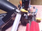
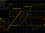
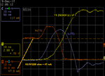
I thought it would be very interesting to look at the amount of overlap of Ic(T1) and Ic(T5) when T1 is turning off, which was one of CataM's concerns.
-Using T5 to provide the 10.5 V faster in order to not wait for the storage time of T1 is a master trick, but I think there is shoot-through for a little amount of time from VS1 through T5 through T1 and ground, isn't it ?

I used two Tektronix CT-6 micro sized current probes for this. So as expected there is some overlap of current (< 30 mA for about 10 ns ) which is not causing any real problems here.
 

Attachments

  • Ic_T1_T5__over2.png
    Ic_T1_T5__over2.png
    70.5 KB · Views: 111
  • Ic_T1_T5__over1.png
    Ic_T1_T5__over1.png
    69.4 KB · Views: 106
  • probes.jpg
    probes.jpg
    78 KB · Views: 95
  • Like
Reactions: CataM

    CataM

    Points: 2
    Helpful Answer Positive Rating
regarding e-design's layout:
What values are the yellow high frequency decoupling caps ?
 

They are 100n ceramic type. The electrolytic is 100uF.
 
  • Like
Reactions: CataM

    CataM

    Points: 2
    Helpful Answer Positive Rating
Here are some more close-up shots showing the tight layout on the pcb.

That's tight, isn't that more like GHz tight? And cool current probe, I want one too. Here's my new layout, I put Vcc on bottom layer and GND on top layer.
IMG_20171210_094922.jpgplane.
Now I'm only one old dented tin can and two BNC's away from RF ;-)

Anyway here are the new measurements with 2n2 instead of FET. Again BLUE trace is the pulse from the pulse shaper 500nS/DIV
Q2(base) DC
Q2b.png
Q4(base) AC
Q4bAC.png
Q1/Q3(base) DC
Q1-3bDC.png
M1(gate) DC
M1GDC.png
 

and secondly I thought that since it's sub-MHz it would be sufficient
That's tight, isn't that more like GHz tight?
The frequency does not have anything to do in this specific application. It is the ON time pulse width and rise and fall times of the control source what is important here.
Even with a 1 Hz frequency square wave signal with 50 ns ON time, your first layout would not work because of high stray inductances. The ON time is so short, that those high stray inductances would not allow the signal to propagate.

Duly noted, I guess I can be forgiven for thinking that, since rise/fall times usually follows frequency. Now that I have the thumbs up for my layout I will start by addressing the Q4(base), Vcc-0.2V is not enough to turn Q4 on..
 

I see that you have the 330 ohm on the base to GND. I mentioned in one of the earlier threads that I left that out as it caused unwanted ringing on the output pulse. Try to see if it improves your pulse shape.

Furthermore, I ended up leaving out R6 (330 ohm) on the base of 2N3904 as it caused unwanted ringing on the output waveform.
 

I see that you have the 330 ohm on the base to GND. I mentioned in one of the earlier threads that I left that out as it caused unwanted ringing on the output pulse. Try to see if it improves your pulse shape.

Sorry, I somehow misread that as you changed value to 330Ω. I have now removed it and indeed the majority of the ringing disappeared especially on Q4(base). But it was not enough to make Q4 open, so I removed R7 (3.3KΩ) completely and changed C2 to 330pF, then Q4 base went down to Vcc-2V and then the 10V->0V pulse became visible on FET gate. But I think I will wait with my celebration until tomorrow when my new scope arrives, and then I can provide pristine scope shots (I'm getting a little bit tired of my old scope for this application, it's a 10 years old 5MHz PicoScope whith cheap probes)
 

I feel you need faster transistors for Q2 and Q4 after looking at simulation plots.

The 2N3904 has a minimum fT of 300 MHz, while the BC337 lists a typical spec of 210 MHz. This seems to be evident in the simulation results. These larger transistors look more sluggish to turn on and off, with more overlap current. They appear to be adequate for the last driver stage. BTW, BC639/640 will also be another good alternative for the driver pair.

Using a BC558/548 combination may be a better choice.

- - - Updated - - -

I removed R7 (3.3KΩ) completely and changed C2 to 330pF

Be careful about increasing this value as it will demand more peak current from your input pulse source.

Below show plots with using BC548/558.
 

Attachments

  • 2N_vs_BC.png
    2N_vs_BC.png
    39.9 KB · Views: 92
  • bc548.png
    bc548.png
    20.5 KB · Views: 91
  • Like
Reactions: CataM

    CataM

    Points: 2
    Helpful Answer Positive Rating
I feel you need faster transistors for Q2 and Q4 after looking at simulation plots.

The 2N3904 has a minimum fT of 300 MHz, while the BC337 lists a typical spec of 210 MHz. This seems to be evident in the simulation results. These larger transistors look more sluggish to turn on and off, with more overlap current. They appear to be adequate for the last driver stage.

Using a BC558/548 combination may be a better choice.

Thank you. I will try that tomorrow when I'm able measure the difference.

Be careful about increasing this value as it will demand more peak current from your input pulse source.

Yes I noticed that, I think I will return to 220pF, it didn't do much difference anyway.

Below show plots with using BC548/558.

Thank you. I'll try the BC558/548 combo and revert.
 

We can see that the speed-up capacitors is essential to get fast switching, but it puts a load on the input signal which distorts the shape. For this reason, you don't want to increase these values if you can avoid it.

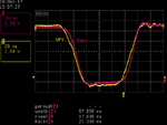
Expanded overlay of VF1 and Gate pulses, show very good tr(18 ns) and tf(22 ns) times, which is close to the simulation results.
 

Attachments

  • speed_cap.png
    speed_cap.png
    24.1 KB · Views: 96
  • 100n.jpg
    100n.jpg
    81.9 KB · Views: 104
  • r_f_gate.png
    r_f_gate.png
    13 KB · Views: 98
  • sim_gate.png
    sim_gate.png
    23.5 KB · Views: 86

We can see that the speed-up capacitors is essential to get fast switching, but it puts a load on the input signal which distorts the shape. For this reason, you don't want to increase these values if you can avoid it.

Expanded overlay of VF1 and Gate pulses, show very good tr(18 ns) and tf(22 ns) times, which is close to the simulation results.

C2 is back to 220p. Q2 is BC548 and Q4 is now BC558.

Oh, and I didn't get my new scope today, apparently for Siglent "next day shipping" means "You'll get it when you get it, so be happy with that". So here are some less than perfect scope shots.

Q2(base) AC
Q2bAC.png
Q4(base) AC
Q4bAC.png
Q1/3(base) DC
Q1-3bDC.png
M1(gate) DC
M1gDC.png

Next, I believe it's time to apply some load.
 

About your input pulse:

Is plot you are showing of this pulse due to the performance of the scope? It appears that the pulse has almost no plateau time and does not look like your initial specification.
 

Attachments

  • I-P.png
    I-P.png
    19.8 KB · Views: 92

Here are some results switching the load with a **broken link removed** device. The on-resistance is a bit high for this application, but this was at hand. The load is just four 1/4W 12 Ω axial resistors in parallel, so there is some inductive component that we can see the ringing effects of on the Vload trace. Furthermore, the probe GND leads will have some effect as well.

In the last plot, I inserted a 10 Ω series gate resistor. It slows down the switching but reduces the inductance effects to get a cleaner trace.
 

Attachments

  • Vload_3R.png
    Vload_3R.png
    24.4 KB · Views: 92
  • gate_res.jpg
    gate_res.jpg
    94.9 KB · Views: 89

About your input pulse:

Is plot you are showing of this pulse due to the performance of the scope? It appears that the pulse has almost no plateau time and does not look like your initial specification.

Yes and No, I'm confident there is a square-ish looking pulse in there, but I wanted to emphasize the pulse timing/delay which looks really good to me.
 

Here are some results switching the load with a **broken link removed** device. The on-resistance is a bit high for this application, but this was at hand. The load is just four 1/4W 12 Ω axial resistors in parallel, so there is some inductive component that we can see the ringing effects of on the Vload trace. Furthermore, the probe GND leads will have some effect as well.

In the last plot, I inserted a 10 Ω series gate resistor. It slows down the switching but reduces the inductance effects to get a cleaner trace.

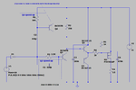
I have updated the schematic to reflect changes.
Screenshot from 2017-12-12 11-38-12.png
Here is the layout
IMG_20171212_111728.jpg
And this is DRAIN on M1
Screenshot from 2017-12-12 11-39-50.png
It's a huge ring though, I would guess it could be attributed to the bulbs since the filament is coiled inside?

- - - Updated - - -

Yes and No, I'm confident there is a square-ish looking pulse in there, but I wanted to emphasize the pulse timing/delay which looks really good to me.

I would like to change my answer to: Yes I believe the pulse looks like that because of the scope/probe performance, despite that - the pulse timing/delay looks really good to me.
 

It's a huge ring though, I would guess it could be attributed to the bulbs since the filament is coiled inside?
And their large leads. Also leads from the other components as well.
If you can (for the components you can), minimize the height above the PCB plane reducing the inductance of the leads.
Also, your layout has improved but is there any problem if you go to a not-so-nice-looking layout like e-design has, tightening more the components together ?
 

Status
Not open for further replies.

Similar threads

Part and Inventory Search

Welcome to EDABoard.com

Sponsor

Back
Top