Continue to Site

Welcome to EDAboard.com

Welcome to our site! EDAboard.com is an international Electronics Discussion Forum focused on EDA software, circuits, schematics, books, theory, papers, asic, pld, 8051, DSP, Network, RF, Analog Design, PCB, Service Manuals... and a whole lot more! To participate you need to register. Registration is free. Click here to register now.

Fast switching transistor with slow rise/fall times, why?

Status
Not open for further replies.
a RDS(on) < 1Ω at the operating voltages indicated
The PMOS below has 190mΩ at 125ºC junction temperature.
I went to 3 amps output current, more than your application needs. The thing is that the Schottky removes about 0.5 V from the already dropped voltage.
 

Attachments

  • PMOSexample.png
    PMOSexample.png
    23.3 KB · Views: 126

For simulations to be more realistic, one should also include the output impedance of the pulse driving source. Assuming an FG will be used then the 50Ω internal resistance must be present in the source setup. When this is not selected most program's default to zero output impedance, which can give overly optimistic results.
 
  • Like
Reactions: CataM

    CataM

    Points: 2
    Helpful Answer Positive Rating
You are right.
I have also included the package inductances (typical values) and the stray inductance might be between complementary emitter follower and MOSFET's gate. Now that explains why I have selected 1 ohm for the gate resistance.
 

Attachments

  • PMOSexampleParasitic.png
    PMOSexampleParasitic.png
    22.5 KB · Views: 131

Here is a design using more old-school parts and keeping the pulse width out, close to the 100 nS of the input pulse. Rise and fall times around 22 nS.
 

Attachments

  • sw_3A_duty.png
    sw_3A_duty.png
    54.3 KB · Views: 149
  • Like
Reactions: CataM

    CataM

    Points: 2
    Helpful Answer Positive Rating
The PMOS below has 190mΩ at 125ºC junction temperature.
I went to 3 amps output current, more than your application needs. The thing is that the Schottky removes about 0.5 V from the already dropped voltage.

Super, thank you. I reproduced it in LTspice, works exactly as it says on the box. BTW when I said "operating voltages indicated" I was in a different place in my mind, where I was using 5v Vcc.

I have some questions though:

1. What's the purpose of the Schottky? If you remove it, it also works fine.
2. I can't quite wrap my head around why it works, because increasing Ids through R3 causes Vds -> Vcc, why is that not causing M1 to shut off prematurely?

- - - Updated - - -

The PMOS below has 190mΩ at 125ºC junction temperature.
I went to 3 amps output current, more than your application needs. The thing is that the Schottky removes about 0.5 V from the already dropped voltage.

Super, thank you. I reproduced it in LTspice, works exactly as it says on the box. BTW when I said "operating voltages indicated" I was in a different place in my mind, where I was using 5v Vcc.

I have some questions though:

1. What's the purpose of the Schottky? If you remove it, it also works fine.
2. I can't quite wrap my head around why it works, because increasing Ids through R3 causes Vds -> Vcc, why is that not causing M1 to shut off prematurely?
 

You are right.
I have also included the package inductances (typical values) and the stray inductance might be between complementary emitter follower and MOSFET's gate. Now that explains why I have selected 1 ohm for the gate resistance.

It seems that the logic gate would have to sink a whopping 143mA, would that constitute a problem when I build it? And can that energy be recovered in the name of efficiency?
Screenshot from 2017-12-03 15-02-44.png
 

1. What's the purpose of the Schottky? If you remove it, it also works fine.
You said (I quote): "i need a MOSFET without the built-in flyback diode"
That Schottky diode cancels the body diode of the PMOS. If you do not need it, you can remove it of course.
2. I can't quite wrap my head around why it works, because increasing Ids through R3 causes Vds -> Vcc, why is that not causing M1 to shut off prematurely?
Increasing IDS does not mean anything. The PMOS is controlled by its Vsg voltage and hence by the control circuitry. Increasing IDS causes more voltage drop on its Rds(on) resistance. Eventually when you have a lot of current, the Vsd will be higher than Vsg-Vth and hence entering into its saturation region which will cause a lot of power loss.

It seems that the logic gate would have to sink a whopping 143mA, would that constitute a problem when I build it? And can that energy be recovered in the name of efficiency?
e-design showed a better proposal in post #24.

@e-design regarding circuit of post #24:
-Using T5 to provide the 10.5 V faster in order to not wait for the storage time of T1 is a master trick, but I think there is shoot-through for a little amount of time from VS1 through T5 through T1 and ground, isn't it ? How did you managed to keep the shoot-through to safe limits ? Moreover, the trick you are using does not have anything to do with the turn off of T1, right ? I mean, giving 10.5 V at the collector of T1 does not help in turning it off faster.. but shoot-through right ?

-I realize now that the T1's pull down resistance has influence in the storage time, which means it helps in the turn off process, can you expand a bit on how do you calculate/"use that resistance"/helps in the turn off process of T1 ? Because the way I see it is that it has negative voltage due to the speed up cap and hence some current is flowing through it back to the source... does that charge come from the base-emitter junction ?

- - - Updated - - -

My post #18 affirmation which I quote is wrong: "R6 has next to nothing of a role in the switching characteristic." -- Wrong affirmation.
 
Last edited:

Increasing IDS does not mean anything. The PMOS is controlled by its Vsg voltage and hence by the control circuitry. Increasing IDS causes more voltage drop on its Rds(on) resistance. Eventually when you have a lot of current, the Vsd will be higher than Vsg-Vth and hence entering into its saturation region which will cause a lot of power loss.

Ahhh, I see my mistake, I mixed up Drain with Source, silly me...

e-design showed a better proposal in post #24.

So I assume you would answer 'yes' to my question, if someone twisted your arm ;-) I'll have a look at it again.
 

-Using T5 to provide the 10.5 V faster in order to not wait for the storage time of T1 is a master trick, but I think there is shoot-through for a little amount of time from VS1 through T5 through T1 and ground, isn't it ?

If you look at the attached plots, you will see that there is no significant overlap of collector currents between T5 and T1. Clearly when Ic(T5) ramps up, Ic(T1) starts ramping down. Looking at Ib(T3/4), shows that almost all of Ic(T5) goes towards driving base current into T3.

- - - Updated - - -

I could have left out R7 (3.3k) for no overlap at all, but then that reduces my peak Ib(T3) current by about 30 mA, which slows down the gate turn-off.
 

Attachments

  • IC_T1_5.png
    IC_T1_5.png
    49.9 KB · Views: 129
  • R7_effect.png
    R7_effect.png
    40.9 KB · Views: 113
  • Iload_var.png
    Iload_var.png
    33.1 KB · Views: 114
  • Like
Reactions: CataM

    V

    Points: 2
    Helpful Answer Positive Rating

    CataM

    Points: 2
    Helpful Answer Positive Rating
Here is a design using more old-school parts and keeping the pulse width out, close to the 100 nS of the input pulse. Rise and fall times around 22 nS.

Thank you. I took the liberty to adapting your design to euro-style. Whether the FET is IRF9131 or FDC5614P or something else, is all exotic to me, I will have to order it anyway.

As part of my understanding, did I divide the sections all right?
Screenshot from 2017-12-04 11-05-00.png

- - - Updated - - -

Here is a design using more old-school parts and keeping the pulse width out, close to the 100 nS of the input pulse. Rise and fall times around 22 nS.

Thank you. I took the liberty to adapting your design to euro-style. Whether the FET is IRF9131 or FDC5614P or something else, is all exotic to me, I will have to order it anyway.

As part of my understanding, did I divide the sections all right?
Screenshot from 2017-12-04 11-05-00.png
 

Watch attachment.

Thank you. What do you mean by BC327 can't withstand driving current? Sim says Ib(Q2)=300mA and Ic(Q2)=1A. According to the datasheet max continuous Ic is 800mA, and this 1A pulsed, shoudn't that work ok? However I can't see max Ib in the datasheet, so could it be that you mean Ib is too high? By how much?
 

I think you are referring to Q1/Q3 in your schematic. Yes, it should be O.K. I was wrong.
 

Here is a design using more old-school parts and keeping the pulse width out, close to the 100 nS of the input pulse. Rise and fall times around 22 nS.

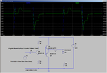
Sorry for the delay, I had some pulse problems, anyway below are the results of the bench test. It's far away from the simulation, but yet I feel it's just a matter of tweaking it a bit, so any tweaking suggestions would be highly appreciated. In all scope shots, BLUE trace is the gate pulse and 500nS/div.

Voltage at Q4(base)
VQ4b.png
Voltage at Q2(base)
VQ2b.png
Voltage at Q1/Q3(base)
Vf1.png
Voltage at M1(drain) I used 3 halogen bulbs in series to achieve 3.5Ω
Vload.png
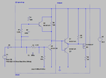
Schematic
Screenshot from 2017-12-08 13-32-46.png
 

BLUE trace is the gate pulse and 500nS/div.

The input pulse or GATE of PMOS?

For initial testing, I would remove the PMOS and temporarily connect a 2n2 capacitor between the gate connection and GND. This will allow you to tweak the circuit to ensure that you get a good-looking gate-drive signal.
Once this is achieved, then start testing with the actual PMOS.
 

Attachments

  • gate_drive.png
    gate_drive.png
    31 KB · Views: 116

The input pulse or GATE of PMOS?.


The input pulse. The gate of the pmos is more or less the same as Q1/Q3(base).

For initial testing, I would remove the PMOS and temporarily connect a 2n2 capacitor between the gate connection and GND. This will allow you to tweak the circuit to ensure that you get a good-looking gate-drive signal.
Once this is achieved, then start testing with the actual PMOS.

Thank you, let me try, then I will revert.
 

Do you have proper decoupling ?
Do you have proper layout ?
Is the ON time 50 ns? Because seems to me that the rise time and fall time of the input pulse is higher than the ON time.

If you add a 1uH inductor in series with the power source in the idealized simulation schematic, almost gives same ringing waveforms... that is why I am asking the above questions.
 

Do you have proper decoupling ?
Do you have proper layout ?

Of course, this would be very important; I agree.

Perhaps you could show us the layout?
 

Here is a small test circuit constructed on a piece of copper clad pcb.
The gate-drive was connected to a 2n2 capacitor to obtain the waveforms, which measured rise/fall times in the 25 ns region. Input pulse came from an Agilent FG set to provide rise and fall times of 50 ns.

Decoupling caps were placed as close as possible (in this case - right on top of the BD135/6)

The gate voltage/current waveforms shows some disturbances due to the insertion of the Tektronix current probe and the resulting stray inductance.

Furthermore, I ended up leaving out R6 (330 ohm) on the base of 2N3904 as it caused unwanted ringing on the output waveform
.
 

Attachments

  • gate_drv2.jpg
    gate_drv2.jpg
    72.2 KB · Views: 111
  • gate_drv1.png
    gate_drv1.png
    61.2 KB · Views: 109
  • probe.jpg
    probe.jpg
    484.6 KB · Views: 104
  • micro_probe.png
    micro_probe.png
    55.9 KB · Views: 99
  • Like
Reactions: CataM

    CataM

    Points: 2
    Helpful Answer Positive Rating
Of course, this would be very important; I agree.

Perhaps you could show us the layout?

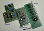
I agree, see below. I did not do it RF-style since I did not have a piece of copper clad board lying around, and secondly I thought that since it's sub-MHz it would be sufficient. However I'm experiencing some scope bandwidth and probe capacitance problems, so I had to order a new scope (Siglent SDS1204X-E) which will arrive Monday, and maybe give me a clearer view.
layout.jpg
 

Status
Not open for further replies.

Similar threads

Part and Inventory Search

Welcome to EDABoard.com

Sponsor

Back
Top