Continue to Site

Welcome to EDAboard.com

Welcome to our site! EDAboard.com is an international Electronics Discussion Forum focused on EDA software, circuits, schematics, books, theory, papers, asic, pld, 8051, DSP, Network, RF, Analog Design, PCB, Service Manuals... and a whole lot more! To participate you need to register. Registration is free. Click here to register now.

Coss related switching losses (Eoss)

Status
Not open for further replies.
When one capacitor is discharging, the same energy is being picked up by the other one, of course, if capacitors were linear.
I don't see how energy can be picked up by a capacitor in a hard switching push-pull configuration. Coss is always charged from Vdc through MOSFET and discharged by MOSFET. I don't recognize a sign error below.

Code:
Esw,tot = Esw1 + Esw2 
        = ∫Coss(V) V dV +  ∫Coss(V)(Vdc - V) dV 
        = ∫Coss(V) Vdc dV
        = avg(Coss(V) Vdc²

or referring to the datasheet quantities Co(er) and Co(tr)
Code:
Esw,tot = Esw1 + Esw2 
        = 0.5 Co(er) Vdc² +
          (Co(tr) - 0.5 Co(er)) Vdc²
        = Co(tr) Vdc²
 

∫Coss(V)(Vdc - V) dV
That integral refers to the second transistor, so at the beginning it was written like
∫Coss(V) *V2 dV2
Then, when you change V2=Vdc-V, why don't change "dV2" as "-dV" ?

- - - Updated - - -

This is what I am saying.
HalfBridge.png
 

In a totem pole arrangement - other factors come into play, even with no load on the midpoint, if you turn on the fets fast, there is a dv/dt impulse on the other fet that causes a small conduction pulse (lowest for -15V on the gate of the off device as Cdg is lowest in this condition).

These effects can easily outstrip any Coss turn on losses - thus the debate is academic at best

For very high frequencies one often has no choice but to go resonant, to eliminate (greatly reduce) turn on losses, and turn off losses...

Under hard switching the lead inductances tend to limit turn on times - giving rise to losses higher than that related to Coss as well.
 
  • Like
Reactions: FvM

    FvM

    Points: 2
    Helpful Answer Positive Rating
Then, when you change V2=Vdc-V, why don't change "dV2" as "-dV" ?
Sign is irrelevant in this case. Either if you are charging or discharging capacitors through MOSFET channel resistance, the loss energy absorbed by the transistor is positive.

In a totem pole arrangement - other factors come into play, even with no load on the midpoint, if you turn on the fets fast, there is a dv/dt impulse on the other fet that causes a small conduction pulse (lowest for -15V on the gate of the off device as Cdg is lowest in this condition).

These effects can easily outstrip any Coss turn on losses - thus the debate is academic at best

For very high frequencies one often has no choice but to go resonant, to eliminate (greatly reduce) turn on losses, and turn off losses...
I agree that there other effects as well. My involvement with the topic is however driven by a real design problem, a high voltage (Vdc = 650V) MOSFET bridge. After optimizing gate waveforms, avoiding the said cross conduction problems, Coss related losses turned out as a relevant problem. The power dissipation could be well matched with Coss datasheet values. In so far, the problem is far from being academic, at least for topologies where soft switching can't be easily achieved.

I'm still desiring a straightforward topology that allows soft switching over arbitrary duty cycles and bidirectional energy flow.
 

dual active bridge will do that - as well as at least one Cuk topology
 

Presume you can achieve ZVS condition in a dual-active bridge by controlling both sides intelligently.

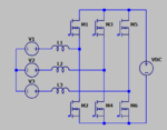
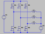
My topology is however an inductive loaded three-phase bridge, either used as active front end or multi-phase buck converter. Suppose ZVS over the full operation range isn't possible without auxiliary switches?

I'm not sure I get your application clearly enough. A multi-phase output could be realized with multiple secondary full-bridges and I wouldn't rule out ZVS operation in such a scenario.

Standard control is phase shift where, with the primary as a reference, the phase of multiple secondaries could be independently regulated.


As you mention most topologies ZVS by relying on load current to some extent which makes it a challenge when duty cycle and current flow changes widely. DAB 'solves' this by choosing the neutral operating point at the top of the circulating current curve. The good news is that load current in either direction can't cancel the necessary ZVS current. The bad news is that circulating current must be 2-4x the maximum theoretical output current.

So that's a huge penalty in circulating losses and magnetics. Yes you can mitigate that by adding another dimension or two to your control..have fun with that (many papers on that subject).


Are you into SiC or Gan yet? This 900V GAN is about to come out, the only >650V I'm aware of:
**broken link removed**
 
  • Like
Reactions: FvM

    FvM

    Points: 2
    Helpful Answer Positive Rating
Sign is irrelevant in this case. Either if you are charging or discharging capacitors through MOSFET channel resistance, the loss energy absorbed by the transistor is positive.
When you discharge a capacitor from Vbus to 0 (Q1) and charge a capacitor from 0 to Vbus (Q2), energy signs are opposed and their quantities are exact the same (absolute value). If you look sharp into the first line of your equation, you can easily see that the result is ZERO assuming linear capacitors.

The only way I arrive to your result, is taking absolute value of the first integral in post #42, which the physical interpretation would be to say: Q1 consumes energy from the Bus source because that means Q1 is again charging ! --> Impossible. Q1 is turning ON which actually discharges energy to the circuit i.e. supplies energy to the circuit from its own charged caps.

If I use "dV" instead of "-dV", for the transition specified (Q1 -> ON, Q2-> OFF), you actually get: Esw= - avg(Coss)*Vbus2, not positive.

Take this equation: "∫Coss(V) V dV + ∫Coss(V)(Vdc - V) dV " and go one step back, which is the first line of my equation in post #42. Can you see that if caps are linear, integrals are canceled out ? First integral is caps energy Eoss1 (in negative) and second integral is energy Eoss2 (in positive), which are cancelling out for equal transistors and linear caps.

Your mistake is that you are saying that the capacitor that is discharging (Q1) is taking energy from the source. One capacitor will take energy from the source to charge itself while the other discharges energy i.e. does not take energy from the source.

The additional energy from the bus that you see is in the overlap loss. If you do not stick only to caps energy, you will see.
 
Last edited:

I'm not sure I get your application clearly enough. A multi-phase output could be realized with multiple secondary full-bridges and I wouldn't rule out ZVS operation in such a scenario.

I'm talking about these two basic applications, 3-phase active front end

afe.PNG

and multiphase DC/DC converter

3p2qs.PNG

CataM, I conclude that you're not fully understanding the purpose of my calculations, it's about determining the Coss related transistor losses. Obviously, the energy stored into a (lossless) capacitor during charge is the same that is recovered during discharge. Also obviously, a resistive switch absorbs exactly this energy amount when discharging the capacitor. But the energy amount dissipated in the charging resistive switch is not necessarily the same, it is only in case of a "linear" (voltage independent) capacitor.

- - - Updated - - -

Are you into SiC or Gan yet? This 900V GAN is about to come out, the only >650V I'm aware of
SiC yes, GaN not yet. Thanks for mentioning the transphorm devices. Particularly regarding Coss, the 900V device can't compete with recent 900V SiC transistors, thus it's no alternative for hard switching circuits.
 

Status
Not open for further replies.

Similar threads

Part and Inventory Search

Welcome to EDABoard.com

Sponsor

Back
Top