Continue to Site

Welcome to EDAboard.com

Welcome to our site! EDAboard.com is an international Electronics Discussion Forum focused on EDA software, circuits, schematics, books, theory, papers, asic, pld, 8051, DSP, Network, RF, Analog Design, PCB, Service Manuals... and a whole lot more! To participate you need to register. Registration is free. Click here to register now.

Buck/Boost Battery Charger works on dummy load, but does not charge batteries

Status
Not open for further replies.
Keep checking between old and new boards - read the data sheet and the app notes carefully ...!

- - - Updated - - -

Two things from the data sheet: 1) if a PowerPath FET is not being used, such as with a lead-acid charging application, connect a 0.1nF capacitor from BGATE to CSN.

2) If the battery voltage is lower than the instant-on threshold (see VFBMIN), BGATE servos the PowerPath FET imped-ance such that a voltage drop between the CSN pin and the BAT pin is created while battery charging continues. If the VCSN – VBAT voltage exceeds 0.4V, maximum charge current is reduced to decrease power dissipation in the PowerPath FET. so at 10A and 0.38V the diss can be 3.8W - enough to kill a fet not heatsunk enough ...

The battery voltage is higher than the instant-on threshold so it's either operating incorrectly or something else is the problem.
(oops my picture did not attach properly in my last post, here it is)
voltages.jpg


VFBmin is 24.7V
Battery voltage is 26.9V.


I just let it run and battery has charged up to 29.035V now (Vfloat is 29.063V)
Charge current is starting to taper off so it's operating in CV mode now and the powerpath FET is still hot enough to burn me. As current decreases, it is getting cooler, but the gate is still not pulled down. I don't think the chip is in instant-on mode, something else must be wrong. My only idea is to try more new P-FETs, I have more coming tomorrow but I don't think it will help. The FET I am using right now was pulled from my old board which worked fine.
 

according to the graph in the data sheet you can have up to 0.5V and 100% I, ( 10A ) this is 5W in the P-fet, even 2W in the P-fet may cook it ...

- - - Updated - - -

also - just looking at your last post the BATT volts are lower than VFB min - aren't they?
 

My battery is at 26.9V right now so the LTC4020 should not be in instant-on mode. Vout is 29.05V when the battery is disconnected (shouldn't it be 31.9V?), and drops to ~27.4V once charging starts.
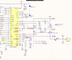
I have double checked the resistor values on R47, 48, 49, 52 and they are populated correctly. I've also measured the voltage at different nodes during charging and they all seem as expected.
**broken link removed**

You are right, the LTC4020 should not be in intsant on mode.
Its also a little bit strange, that the battery float voltage is setup, while the battery is disconnected.
The voltage should be 29.05V while battery is connected and about 31.95V (Vfloat * 1.1) while disconnected.


Maybe your input voltage is dropping?
This could be a problem:
Vin_Reg:
Input Voltage Regulation Reference.
Battery charge current is reduced when the voltage on
this pin falls below 2.5V. Connecting a resistor divider
from VIN to this pin enables programming of minimum
operational VIN voltage for the battery charging function.
This is used to program the peak power voltage for a
solar panel, or to help maintain a minimum voltage on
a poorly regulated input supply. This pin should not be
used to program minimum operational VIN voltage with
low impedance supplies.

I assume that you are using a low impedance high power capable supply?
In the current schematic the divider is 100k to 100k which yields to an regulation voltage of 5V -> quite useless in this setup.
If your power supply is stable and has enough power output this should not affect the charge current regulation loop.
But maybe here are some wrong values soldered or your power supply has massive transients?
You can also complettly disable the VIN_Reg feature by removing R50. (like on the LTC4020 demo board)

If this is not the cause - i would replace the LTC4020...once again.
 
Well spotted Danie.

We all look forward to hearing what clears up the issues ...
 

You are right, the LTC4020 should not be in intsant on mode.
Its also a little bit strange, that the battery float voltage is setup, while the battery is disconnected.
The voltage should be 29.05V while battery is connected and about 31.95V (Vfloat * 1.1) while disconnected.

Okay that is what I thought. Sometimes the float voltage is 31.9 (expected), mostly on initial power up, then after battery is connected and disconnected, float voltage will be 29.05V sometimes, or 31.9V other times.
I'm thinking the P-FET must be damaged, that is why the regulator has 29.05V because the P-FET cannot turn off and when the VFB pin is over 2.5V, it directly changes the converter control loop.

Both P-FETs were working before on other boards. My overnight shipment of new P-FETs was lost so I will not have more until tomorrow now.

Maybe your input voltage is dropping?
This could be a problem:


I assume that you are using a low impedance high power capable supply?
In the current schematic the divider is 100k to 100k which yields to an regulation voltage of 5V -> quite useless in this setup.
If your power supply is stable and has enough power output this should not affect the charge current regulation loop.
But maybe here are some wrong values soldered or your power supply has massive transients?
You can also complettly disable the VIN_Reg feature by removing R50. (like on the LTC4020 demo board)

If this is not the cause - i would replace the LTC4020...once again.


Power supply is very stable, high quality Meanwell 600W supply. I removed R50 like you suggest, but the behavior is the same so it should not be VIN_reg causing problems.

I am using a hot air reflow wand to replace components. Is it possible I have damaged the P-FET by too much heat? I use low heat under the board to warm the board up, then higher heat above the component to reflow solder and remove/replace. The P-FET requires a lot of heat because the connected copper is so large.

Tomorrow morning I will replace the P-FET, all 8 N-FETs and LTC4020 with new parts at the same time to make sure no damaged components are damaging new parts.
 

The new P-FETs are operating correctly now. Both my lost shipment and replacement shipment showed up today so I tried replacing just the P-FET and nothing else and this fixed the overheating issue on both prototype boards.
I used more heat on the underside of the PCB and less heat from the hot air wand to replace this time. I'm not sure if that made any difference but it did take much longer so I think heating was more uniform.

~31.7V with battery disconnected, then drops to VBATT (28.1V right now) when connected. Charging about 9.8A and nothing is burning up. I will still need to test/fix very low voltage battery to see if the instant-on feature kills the P-FET. Lowering the VFB_min should fix that.

Now I can do more testing at full power on the switching converter. The N-FETs are getting slightly warm. I probe the low side sense resistor (RsenseB) and get this current measurement:
DSC_1277.JPG

Vin = 24V
Vout = 28.1V

So it should be solidly in boost mode operating as described:
When VIN is lower than VOUT during step-up (boost) operation, switches C and D perform the PWM required for accommodating power conversion. Ideally, switch A would conduct continuously and switch B would stay off, making PWM switching action much like that in a synchronous boost topology. Since switch A also uses a bootstrapped drive, however, the B switch conducts for 100nS during this refresh period. A 75ns non-overlap period, separates the conduction of the two switches, preventing shootthrough currents.

Is the bootstrap refresh causing the current spike through RsenseB? Possibly due to shoot-through from Switch A to B?

Here is both sides of the inductor under the same conditions if that is helpful:
DSC_1278.JPG


By the way, I have 22R gate resistors installed on this board, and 10R gate resistors on the other board. Both have similar current spikes on RsenseB.
 
  • Like
Reactions: Danie.

    Danie.

    Points: 2
    Helpful Answer Positive Rating
In boost there should be no current in RsenseB - which is roughly what you see I think ... only the refresh ... else A could not stay on indefinitely ...

glad to see things are working virtually as intended (?) - well done ..!
 

When Switch B turns on and SW1 node (ch2) goes low, it seems Switch C also turns on and SW2 node (ch1) goes low, pulling down both sides of the choke at the same time, this is normal?
At the same time, it looks like current flows from GND into SW1 (peak is -86mV/5mR = -17.2 A) then current reverses and flows from SW1 into GND (peak is 120mV/5mR = 24 A).

The FETs at Switch A and Switch D get fairly hot, but not unsafe. About 65 deg C. I think it should run cooler.

I changed the gate resistors from 22R -> 4R7 and temperature is now around 43 deg C. RsenseB current spike is much higher, but temperature is lower so I guess this is good.

I think now I will order parts to populate 2 more boards with all new values and verify everything works with new parts.

Big thanks to you guys and all the ideas to try!!
 

sounds like the refresh for the bootstrap gate power is happening on both sides at the same time (?)

lowering Rgate with give you bigger current spikes and worse EMC performance but gain efficiency - best to use the best fets you can with fairly low Rds-ON so that they can soak up some turn on losses - a reverse schottky across Rgate will give fast turn off which is usually a good thing ... 22E for on, 40V 1A schottky for off ...
 
We look forward to some full power wave-forms..! - when the Batt is < 11 volts, the turn off Vds looks good - by which I mean there must be some good caps close to the fet action ...
 

Status
Not open for further replies.

Similar threads

Part and Inventory Search

Welcome to EDABoard.com

Sponsor

Back
Top