Continue to Site

Welcome to EDAboard.com

Welcome to our site! EDAboard.com is an international Electronics Discussion Forum focused on EDA software, circuits, schematics, books, theory, papers, asic, pld, 8051, DSP, Network, RF, Analog Design, PCB, Service Manuals... and a whole lot more! To participate you need to register. Registration is free. Click here to register now.

Buck/Boost Battery Charger works on dummy load, but does not charge batteries

Status
Not open for further replies.
I must say congratulations. I can remember when you almost gave up. It's good you listened and then gave that little final push that you needed to succeed when we all advised.

One major thing that I have realized with the initial calculations is that we were treating your project as if it were an adapter. We should have considered that at the output of a charger we have both an opposing voltage source and a load resistance in series with it. This means that for the required output current, we will have:

Rload=(Vout-Vbatt)/Ichg.

So designing this as an adapter, we have:

Iout = Vout/Rload.

This makes the design output current of a charger way higher than that of an adapter for the same design spec.

From the Ichg value, we could calculate peak and average switch currents to determine the sense resistors. So for a charger the sense resistor would definitely be smaller.

Congrats once again on your success!
 

I finally have my new design of the battery charger prototyped and it seems to have more switching issues. When allowed to run at full load, it makes hissing/squeeling noises and everything gets hot very quickly (capacitors, fets, choke)

It is stable at light load (~3A output), but the diode D3 gets very warm. I've removed it (because it is not installed on the demo board) and the MOSFETs Q8 and Q9 get warm.
Here are my switching components:
rev2.jpg

My nominal setup is Vin= 24.0V, Vbatt= 28.9V (CVmode) so the 4-switch converter should be operating in boost mode where Q8/9 and Q6/7 are being modulated.

The gate waveforms all look normal except for TG2 (gates of Q8 and Q9). Here is TG2 (CH1-yellow) and SW2 (CH2-blue). They are basically identical waveforms.
DSC_1215.JPG

As the load increases, the oscillation before the gate drops happens sooner in the pulse and more frequently. The oscillation is occurring for 2 cycles each time and happens every 6-7 cycles. This must be something to do with the control loop?

Also if I probe the low side sense resistor there is a lot of ringing during the switching of Q1/2 and Q4/5
This is S-BOT (over the low side sense resistor R2) on CH1 and SW1 on Ch2 (blue)
DSC_1216.JPG

Obviously something is quite wrong, any ideas where to look next?
 

If D3 gets warm then the associated fets are not doing their job - very hard to help any further from a distance - but layout is everything - compare to your old lashup and see what is worse ... or different ...

- - - Updated - - -

before it was all to do with the current sensing - is your control IC any closer to the power switching? also - slowing the turn on of the fets lowers noise and allows the control ckt to do it's thing in a little more peace and quiet ... - worth a try ...

- - - Updated - - -

Also - some fets just do not like running in hard parallel - at least 10E to each gate ...

- - - Updated - - -

picture of actual hardware with close ups around I sense and tracks to IC / filtering ...
 

By doing their job, what do you mean? The FETs associated with D3 are the same in the waveform I attached and the waveform at SW2 matches the waveform of the gate drive.

I left 0ohm jumpers for gate resistors, I can try 22R resistors there to see if there is improvement.

It is hard for me to diagnose the problems at higher current. I have to use a larger, non-isolated supply (common is tied to earth at the wall) and when I am using that I cannot attached the scope reference clip to anything or I get large ground loop noise. I have been able to scope some things at high current but mostly I have to diagnose at lower current which is difficult.

Here are some images that may help:

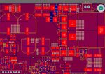
This is the switching components layout:
rev2_switching.jpg

Here are the internal layers with some planes labeled in red. You can see the inductor current sense traces (blue) on Layer 4, kelvin connected on layer 1 and the gate traces (orange) on Layer 3. They are routed such that the sense traces have continuous ground planes on adjacent layers above and below (L2 and L3).

SGND and PGND are connected at a single location on L3 circled in green. This is exactly how the demo board is. The current sense traces on the adjacent layer pass under where they are tied together so there is never a break in the plane.

rev2 layers.jpg

Here is a picture of the board populated
DSC_1217.jpg

- - - Updated - - -

Also, here is a close-up of the filtering of the current sense at the IC with the differential input pins shown. Left is 3D render, right is 2D with pads labeled.
filtering.jpg


Here is the schematic
filtering_sch.jpg

I currently have removed the Y-caps C39, C40, C41, C43 and increased C44 and C45 to 1uF but it did not make any changes so far.
 

C39, 40, 41,43 would seem to be useful if fitted - worth trying before posting.

I see the gate drive lines are more or less under the I sense lines

I think you will have to invest in a decent power supply so you can vary the input volts easily and have plenty of current - but with a current limit ....

that way you can use your scope to probe around - put as many turns of the scope lead as you can thru a hi-mu toroid - a 1k res in the probe tip is of use sometimes too ( short leads )

- - - Updated - - -

worth trying putting a flux band around the choke and tying it to power gnd - just to see if it helps...
 

I just dropped by to see how you manage to evaluate :

1) the deadtime control in relation to L/R decay time a fly back diode is slow from low V, low R but a Zener diode (high V allows for faster dI/dt recovery)


2) Spectral Response driving almost a short circuit.

The ESR , DCR RdsOn effects as when you are driving a battery the equivalent AC impedance is the ESR and ESL which with source caps ESR and FETs Ron, may give rise to high Q series-resonances and sub harmonic squeals from ceramic/ferrite piezo effects. It helps me to evaluate Bode plots of all parasitic non-ideal properties.

I use Falstad frequency response and add all ESR’s, ESL to get a rough idea. But mutual coupling and crosstalk is harder to simulate with such a complex board. Coiling your 10:1 coax helps a bit but not as much as a CM ferrite clamp for > CM rejection of stray Currents > 20MHz.

In the end comparing differences in your layout and part selection from the Eval PCB “may” reveal some clues.

Good luck.

- - - Updated - - -

Hi,
I have built an LTC4020 basically identical to the DC2134A evaluation board.

What are the significant differences in part numbers and layout? Both are critical choices.
 

EP,
Could you explain what the point is of having a high and a low sense resistor for the inductor? Most of the examples and similar circuits I've looked at and read about only have a single sense resistor shared by both half bridges.

Is the current sense measurement being used in the control loop in any way? I had thought it was simply for overcurrent protection of the inductor and circuitry. I thought the voltage output was measured by the control chip and the duty cycle was varied to regulate the output.

The Y-caps were fitted on both of my prototypes and I removed them on one to see if it made any improvement.

The high side fets Q1/2 on the input have blown up now and the board has a direct short from VIN to PGND I think the 4020 chip may be dead as well, I'm waiting on parts to repair it. This happened at startup with no load connected on one board. What could cause the high side FET to fail?

I'm using SIR688DP-T1 FETs for all 8, same as the first 2-layer board version that worked (okay-ish) after filtering the current sense inputs.
A lot of example and eval boards use different MOSFETs for the input side and output side. What's the reason for that? I assumed input side needed higher VDS max than output side so it's more cost effective.
The eval board from LTC uses SIR664DP (60V, 60A) on the input side and SIR422DP (40V, 40A) on the output side.


The main differences between the eval board and my prototype are switching component selection. Mainly the choke, capacitors, MOSFETs and reverse recovery diodes so any feedback on my switching component selection would be extremely appreciated. This is my first high power synchronous circuit so I have little experience selecting power electronics components. Generally I am used to very low power digital circuits so I appreciate all the help!
 

check your schematic / new board for basic errors - e.g. wires crossed over - you may have cooked or cracked a chip R or C in the new build - if the new build is identical to the old board that worked - there must be a basic cause for inoperability ...
 

check your schematic / new board for basic errors - e.g. wires crossed over - you may have cooked or cracked a chip R or C in the new build - if the new build is identical to the old board that worked - there must be a basic cause for inoperability ...

The main component differences between last rev and this rev are more input and output capacitance with higher Irms ratings because capacitors were getting warm at full load. Also the improvement in layout going from 2 layer to 6 layer for better noise immunity on the current sense by running on internal layers.

I'm looking for basic errors on the board like damaged chips or solder shorts but I need some area to focus on.

I have one prototype working again. The gate of high side output FET again does not look normal, it still looks like this:
DSC_1215.JPG

Here is what the above is looking at:
DSC_1215_sch.JPG

Is this expected or is there something wrong with TG2 gate drive during boost mode? The ringing seen in the ON portion of the waveform happens every 6-7 cycles and changes in how much of the ON portion as the load increases and decreases. It looks to me like the LTC4020 is floating the gate for a portion of the cycle. Is it doing this because of errant readings on the current sense during that portion of the cycle? The other 3 gates look nice and clean. I can scope 2 gates at once if that is helpful?
This really all boils down to I don't know what the waveforms are supposed to look like under normal conditions.

At very light load (~50-100mA) the converter seems to go into some kind of pulse skipping mode.

- - - Updated - - -

Here is a video clip of the oscilloscope of what I'm looking at for TG2 and BG2.

https://imgur.com/a/HjndgIK

Probe locations:
MOV_1220_sch.jpg
 

Is the current sense measurement being used in the control loop in any way? I had thought it was simply for overcurrent protection of the inductor and circuitry. I thought the voltage output was measured by the control chip and the duty cycle was varied to regulate the output.

According to the functional schematic, the measurement is compared with the charge controller ITH output and the difference controlling the pulse width. The large Isense filter time constants implemented in your design will surely affect circuit operation. An LTspice simulation can be a suitable way to better understand these effects.

I see that the filter seems to be necessary to make your circuit work, but it's quite different from the time constants used in the suggested circuit and eval boards.
 

please post the schematic of the control loop bits - as it is built right now - I suspect a poorly soldered R or C - or cooked/cracked C or wrong value some where ...

also - did you try the flux band around the choke? even 4 turns of insulated wire with the ends shorted will suffice for a noise reduction test ...

- - - Updated - - -

the video looks fine - you are not over driving logic level fets ... ?

- - - Updated - - -

have you put 22R on each fet gate ?
 

According to the functional schematic, the measurement is compared with the charge controller ITH output and the difference controlling the pulse width. The large Isense filter time constants implemented in your design will surely affect circuit operation. An LTspice simulation can be a suitable way to better understand these effects.

I see that the filter seems to be necessary to make your circuit work, but it's quite different from the time constants used in the suggested circuit and eval boards.

Do you mean the component selected for ITH and Vc pins? I used the same value as the Eval board, however those are different from the values in the typical application so I was not quite sure what to use.
filters.jpg

I have gotten one board working again (replaced Q1/Q2 and removed D2) Here is exactly how it is currently fitted:
rev2_schematic.jpg

I replaced R20, R21, R23, R34 (10 ohm) with 0 ohm jumpers and I think it has fixed the stability problem and does not explode FETs now.

I noticed at power up, if the current limit is up too high on the power supply, it immediately shorts Q1/2. If the power limit is set lower, it blips the CC limit faster than I can see and starts up okay. But with no current limit on my CV supply, it explodes Q1/2.
Now, without the 10 ohm series resistors on the current sense, it starts up without an external current limit. The Y-caps are still in place.


The converter seems to be running okay now, but with the battery connected and high power supply, the powerpath P-CH MOSFET (Q11) for the battery charger is getting very very hot instantly and the battery only receives about 5-6A.

VGS for the SI7145DP is +/-20V and I'm wondering if this is enough? It matches the eval board SIR688DP which has the same maximum VGS, however the eval board maximum converter voltage is 28V and mine is 29.1V.

With the gate pulled low by the LTC4020's BGATE pin, won't this exceed the maximum -20V Vgs? Is it possible the P-FET is being damaged?
 

Slow the soft start down so it takes ~2 sec to start, use the values in the app note for the control loop - i.e. the slower ones
 
Last edited:

Slow the soft start down so it takes ~2 sec to start, use the values in the app note for the control loop - i.e. the slower ones

Received replacement chips today and have the board working again.

I have 1uF on both inductor soft start and battery charge soft start. I've ordered the capacitors required to slow down the control loop from the app note.

The switching converter seems to be functioning correctly, it is the powerpath control that is behaving differently than my first rev now.
The first rev had no problems at 10A charging, the P-FET got slightly warm but not hot.

On this rev, the P-FET gets extremely hot in seconds. When the battery is connected, the gate isn't being pulled down, Vgs is only about -400mV which is far below the SI7145DP's -2.3V gate threshold.

I'm pulling off and touching up the resistor feedback components but so far I haven't found anything abnormal so again I'm stumped.
Any suggestions on how to troubleshoot the P-FET gate not being properly pulled down? This is the 2nd board with this exact same problem.
 

bad parts? could put a 2k2 from g-source on the P-fets - just to help out ...

slowing the soft start should help to find the p fet problem ... keep comparing to original lash up - use your eyes - look for differences ...

- - - Updated - - -

Bad P fet ...
 
Yup, I have replaced the P-FET with one I pulled off my old board. Battery now receives 9.7A (designed at 10A) but still gets very hot.
The gate is still only being pulled down for a Vgs about -2.0V so R_on is still too high.

My guess is the damaged P-FET also damaged the gate drive of the new chip and I need to replace both the LTC4020 and P-FET at the same time. I'll need to order more P-FETs, I'll report back once I replace both. I can only fry so many LTC4020's - they are quite expensive.

Is it reasonable to use a P-FET with max Vgs +/- 20V and max Vds of -30V? It seems if the LTC4020 pulls the gate down to 0V, Vgs will be -28V. Is this an oversight of the Eval board design or does the chip protect the gate from damage?

Is there a way to protect the FET gates to make this design more robust? I followed the app notes and have the P-FET connected directly to the chip. Reliability and robustness is more important than component cost of this design.

Thanks
 

you can put a zener on the P Fet and a current limiting resistor in series to the gate - ( 28-15 )/10mA = 1k3, say 1k5 - it doesn't need to turn on/off fast ?
 
What voltage does the battery have in this case?
Maybe this is the instant-on feature of the LTC4020? Set by R48 and R49.
With the populated values (R48 = 24k; R49 = 255k) you should get:
Vmax ~ 31,96V
Vmin ~ 24,70V

So if the battery is below Vmin the LTC4020 regulates the BGATE pin to get a voltage drop of 0.4V from CSN to BAT (= FET).
This results in a total power disipation of ~4W in the mosfet.
According to the datasheet of the SI7145 this is outside the safe operating area (see page 4) .
It seems that this is also the reason, why Analog sets the max. charge current to 6.25A -> close to the safe zone

Hope this could help a bit!
 
you can put a zener on the P Fet and a current limiting resistor in series to the gate - ( 28-15 )/10mA = 1k3, say 1k5 - it doesn't need to turn on/off fast ?

I looked back in the datasheet and there is a brief mention in pin description of BGATE that the pin is internally limited to CSP-BGATE = 9.5V so a P-FET rated for Vgs +/- 20V max should be fine.
It can turn on/off slowly, so I will include pads for a gate resistor when I order more. Thanks


What voltage does the battery have in this case?
Maybe this is the instant-on feature of the LTC4020? Set by R48 and R49.
With the populated values (R48 = 24k; R49 = 255k) you should get:
Vmax ~ 31,96V
Vmin ~ 24,70V

So if the battery is below Vmin the LTC4020 regulates the BGATE pin to get a voltage drop of 0.4V from CSN to BAT (= FET).
This results in a total power disipation of ~4W in the mosfet.
According to the datasheet of the SI7145 this is outside the safe operating area (see page 4) .
It seems that this is also the reason, why Analog sets the max. charge current to 6.25A -> close to the safe zone

Hope this could help a bit!

Danie, thanks for the response. I think you are right with what is happening but it does not explain why. When I plug in the battery (just for 10 seconds before the powerpath FET explodes), I can measure Vds on the P-FET as ~ -0.475V

My battery is at 26.9V right now so the LTC4020 should not be in instant-on mode. Vout is 29.05V when the battery is disconnected (shouldn't it be 31.9V?), and drops to ~27.4V once charging starts.
I have double checked the resistor values on R47, 48, 49, 52 and they are populated correctly. I've also measured the voltage at different nodes during charging and they all seem as expected.
**broken link removed**

My first board had slightly different resistor values for a charging CV of 29.4V (4.2V/cell) however I have changed them on this version for a CV of 29.05V (4.15V/cell) for less battery stress.
I've ordered the resistors I used on my last board (20k and 215k) and will see if that changes things, otherwise I have no idea why the chip is trying to regulate BGATE.

Is there a way to disable instant on mode in design? I do not think it has much use for me, my Vout can be as low as 14V.
Or do I need to separate the VFBmax and VFBmin resistor dividers so that VFBmin can be less than 24.7? It looks like trickle charge is set by the VFB pin, so it will not affect that feature.

So I need to select a select a FET capable of dissipating heat at -.45V Vds at 10A (4.5W) and lower my VFBmax divider.

This still doesn't explain why I have 2 prototype boards using the powerpath FET as if it were in instant-on mode.
 

Keep checking between old and new boards - read the data sheet and the app notes carefully ...!

- - - Updated - - -

Two things from the data sheet: 1) if a PowerPath FET is not being used, such as with a lead-acid charging application, connect a 0.1nF capacitor from BGATE to CSN.

2) If the battery voltage is lower than the instant-on threshold (see VFBMIN), BGATE servos the PowerPath FET imped-ance such that a voltage drop between the CSN pin and the BAT pin is created while battery charging continues. If the VCSN – VBAT voltage exceeds 0.4V, maximum charge current is reduced to decrease power dissipation in the PowerPath FET. so at 10A and 0.38V the diss can be 3.8W - enough to kill a fet not heatsunk enough ...


- - - Updated - - -

and: During the majority of a normal battery charge cycle, the LTC4020 makes a low impedance connection between the battery and the DC/DC converter output through the PowerPath FET, as in Figure 3. This PFET is controlled by the LTC4020 through modulation of the BGATE pin, which is connected to the FET gate. When charging is disabled, the FET is disabled, disconnecting the battery from the converter output by pulling the gate of the PowerPath FET high via the BGATE pin. The converter output is regulated by VFBMAX while the FET is disabled. When normal charger operation resumes, the gate is pulled low. As the BGATE pin is a slow-moving node, C/10 detection is disabled until the BGATE pin approaches its normal operating voltage, which prevents premature C/10 detection during reconnection of the battery. The slow movement of BGATE can also cause the converter output to regulate to VFBMAX for a short time during start-up until the FET is enabled. This FET is also linearly controlled during low battery conditions to enable the instant-on function, where the converter output can be separated from a heavily discharged battery to power the rest of the system before the battery voltage responds to charging. C/10 detection is also disabled when the charger is operating in instant-on mode.

- - - Updated - - -

and: In CC mode, the LTC4020 will maintain full programmed charge current capability for the duration of the timer period. The trickle charge function is disabled, although maximum charge current will be reduced during lower deck operation if there is excessive voltage (>0.3V) imposed across the PowerPath FET. The charger will terminate the charge cycle and the PowerPath FET will become high-impedance once timer EOC is reached.

- - - Updated - - -

and for the IC: The LTC4020 is typically biased directly from the charger input supply through the PVIN and SENSVIN pins. This supply provides large switched currents, so a high quality, low ESR decoupling capacitor is recommended to mini-mize voltage glitches on the VIN supply. Placing a smaller ceramic capacitor (0.1μF to 10μF) close to the IC in parallel with the input decoupling capacitor is also recommended for high frequency noise reduction. T

- - - Updated - - -

and for the o/p: Output Decoupling During periods when the LTC4020 DC/DC converter output is not connected to the battery through the PowerPath FET, the system load is driven directly by the converter. The converter creates large switched currents, so a high quality, low ESR decoupling capacitor is recommended to minimize voltage glitches on the VOUT supply. Placing a smaller ceramic decoupling capacitor (0.1μF to 10μF) in parallel with the output decoupling capacitor is also recommended for high frequency noise reduction. The VOUT decoupling capacitor (CVOUT) absorbs the majority of LTC4020244020fdFor more information www.linear.com/LTC4020the converter ripple current, so it must have an adequate ripple current rating. RMS ripple current (IΔRMS) is highest during step up operation, and follows the relation: ...

- - - Updated - - -

and again Bgate: If the battery voltage is below a programmed minimum operational output volt-age, corresponding to VFBMIN = 2.125V, the PowerPath FET is configured as a linear regulator, allowing the DC/DC converter output to rise above the battery voltage while still providing charge current into the battery. During instant-on operation, the BGATE pin is driven by theLTC4020 to maintain the minimum programmed voltage on the PowerPath FET source, the FET acting as a high impedance current source, providing charge current to the battery, independent of the battery voltage.

- - - Updated - - -

and: in certain applications, the PowerPath function is not required. For example, lead-acid chargers do not termi-nate (they remain in float charging mode indefinitely), so the battery need never be disconnected from the output, provided the instant-on feature is not desired. The PowerPath FET can be eliminated in these applica-tions by tying the CSN side of the sense resistor to BAT, connecting VFBMIN to ground, and connecting a 100pF capacitor from the BGATE pin to CSN. See Typical Ap-plication Circuits section.

- - - Updated - - -

also see fig 20 of data sheet.
 

Status
Not open for further replies.

Similar threads

Part and Inventory Search

Welcome to EDABoard.com

Sponsor

Back
Top