Continue to Site

Welcome to EDAboard.com

Welcome to our site! EDAboard.com is an international Electronics Discussion Forum focused on EDA software, circuits, schematics, books, theory, papers, asic, pld, 8051, DSP, Network, RF, Analog Design, PCB, Service Manuals... and a whole lot more! To participate you need to register. Registration is free. Click here to register now.

Increasing OpAmp output current

engr_joni_ee

Advanced Member level 3
Joined
Nov 3, 2018
Messages
822
Helped
2
Reputation
4
Reaction score
7
Trophy points
18
Activity points
6,877
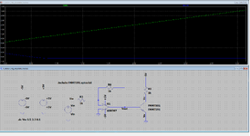
The input to the OpAmp is 0 to 3.3 V. I am using OpAmp in unity gain inverting configuration. The output of the OpAmp will be 0 to -3.3 V. The problem is that the output current of the OpAmp I have selected can not deliver 500 mA if a load is connected. I know that there are OpAmp with higher output current but for some reason, I need to find a solution with FMMT591 OpAmp. One option is to buffer the output using a transistor to increase the output current. I am using PNP at the output of OpAmp. The schematic is attached. Kindly have a look and suggest how can I get 0 to -3.3 V at the load that require 500 mA. Note that the input of the OpAmp will be controlled by DAC/FPGA to get adjustable power supply at the load.
 

Attachments

  • Untitled 738.png
    Untitled 738.png
    48.1 KB · Views: 156
Last edited:
The simulation circuit makes no sense. Vout is clamped by FMMT591 base-emitter diode, increasing Iout would only burn the transistor. Ib absolute maximum is 200 mA.
I guess you are intending something different but what is it?
 
Hi,

What is the "output" you want to regulate?

R6 is the feedback resistor.
Basically this resistor needs to be connected to the node you want to regulate.
Currently it is connected to V_out (Which implies this IS your output)

Now, if R6 is not connected to V_out then there may be gain/phase shift that influences the OPAMP stability.
If you encounter ringing/oscillation, then add a capacitor (start with 1nF) from V_out to -In

****
Some phrasing corrections:

You say "the input to the OPAMP is 0..3.3V". This basically is not true. Both Opamp inputs will be close to zero. Always. So to be exact you may say "the input is 0..3.3V" or the "OPAMP_circuit_input is 0..3.3V".
--> it makes a big difference when you read the datasheet regarding "input voltage range". Here 0V applies.

You say "unity gain". This is not true either. Unity gain means A = +1. While in your case A = -1.
--> it makes a big difference when reading the datasheet according stability. There are OPAMPS that are stable at A=-1, while they are not stable at "unity gain".

You say: "I need to find a solution with FMMT591 OpAmp".
--> But the OPAMP name is AD8397.

***
To the schematic:
* missing power supply decoupling capacitors
* missing low pass filtering
* the BJT circuit should be drawn upside down, in a way it meets the standard "positive voltages are up, while negative voltages are down".
* you can never have 500mA through R1. It needed 500V...
* AD8397 is a dual OPAMP: mind to not leave unused inputs floating and keep output in regulating state
 
Sorry, the OpAmp is AD8397. To simplify I just simulate inverting OpAmp output. The input is 0 to 3.3 V and the output is 0 to -3.3 V.

The load requirement is 500 mA with a variable voltage 0 to 3.3 V. The OpAmp AD8397 we selected can not deliver that much current. Can a push-pull stage using PNP and NPN solve the problem ?
--- Updated ---

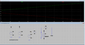
I also simulated push-pull stage separately. The transistors PNP and NPN can work at 500 mA. I am wondering how can I combine this push-pull with the OpAmp. So that I get variable voltage between 0 to -3.3 V on the load.
 

Attachments

  • Untitled 739.png
    Untitled 739.png
    43.4 KB · Views: 90
  • Untitled 740.png
    Untitled 740.png
    70.5 KB · Views: 89
Last edited:
You will find in attached several boosted designs and considerations.

Also your booster stage will add phase shift reducing phase margin so you
will have to compensate it for that, also discussed in ap note.

Does your output have hi C load ? More phase shift to address.


Regards, Dana.
 

Attachments

  • an47fa.pdf
    5.1 MB · Views: 90
The load requirement is 500 mA with a variable voltage 0 to 3.3 V. The OpAmp AD8397 we selected can not deliver that much current. Can a push-pull stage using PNP and NPN solve the problem ?
Basically yes. Did you try to combine AD8397 with BJT booster, closing feedback loop around the output stage? A base-emitter parallel resistor of e.g. 20 to 50 ohm can force the circuit into class-AB operation with less crossover distortions.

Load parameters haven't been specified yet apart from 3.3 V/500 mA rating, also no dynamic requirements (bandwidth, rise/fall-time) at all.

Assuming a resistive 6.6 ohm load, FMMT591 power rating would be exceeded by a factor of nearly two in worst case operation point Vout = 2.5 V. Or is average output current much lower than 500 mA?
 
If your BW is <1MHz but you must have 0 to 3.3V @ 500 mA and not exceed the power limit of the transistors then more specs are needed on the load reactance. The source impedance, Zout (f) must be much lower than Zload(f) for a good damping ratio just like audio woofer amps.

If you can supply +/- 5 that wastes too much power and bandwidth so ideally if you can supply -1.25V (typ LDO) and 5.0 V then you can drive the complementary pair with feedback from the output. consider a large copper area 2 x 2cm heat on each collector and avoid any parasitic positive feedback at all costs. The high slew rate error correction will overcome the Class B drivers with minimal power loss in the OP AMP.

Now realize you must use use larger package transistors than SOT23 to dissipate 3W into a 10W heat sink to reduce the Tj rise from 100’C to something a lot cooler. The large BJT’s also add diode junction capacitance which determines your maximum slew rate from V/RC. Also removing the heat loss in the PNP has just moved it to your negative LDO if you were planning on -5 Vin. (!) But these are the compromises you make with a fixed choice of R2R Op Amp.

Please define all missing assumptions.
Slew rate
 
Last edited:
I will look more in to this circuit. The load voltage requirement is 0 to -3.3 V. I forget -ve sign in #4.

A general question regarding power limit of a BJT transistor. If the biasing voltages are at +5 V and -5 V as shown in my push-pull simulation, and we have a load connected to the BJT transistor requiring 0 to -3.3 V and 500 mA continuous current. Are we exceeding the power limit of transistor ? How we can calculate the heat dissipation for this particular example.

I will come again on combining AD8397 with BJT booster.
 
Last edited:
How we can calculate the heat dissipation for this particular example.
It´s the same for any (non storage and non power converting) device:
--> P = V x I
that´s it.
V = the voltage across it, I = the current through it.

One of the most basic formula in electronics.
I guess I have already told you several times before.

Klaus
 
The PNP transistor will only react to negative swings, you need a NPN to the output too - both need to be biased, otherwise they will work in their non-linear region, the last thing you want from a linear device such as op amp based circuit :) In short you would need a biased bipolar output stage because your output from the op amp is bipolar too.

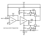
Attached is an example of a biased bipolar output stage inverting and simple (1) and non-inverting (2)- only would use a modern op amp and modern transistors and it should be all good.

What is the desired bandwidth of the circuit?
 

Attachments

  • Bild 13.06.24 um 18.15.jpeg
    Bild 13.06.24 um 18.15.jpeg
    128.3 KB · Views: 69
  • Bild 13.06.24 um 18.27.jpeg
    Bild 13.06.24 um 18.27.jpeg
    182.2 KB · Views: 69
Last edited:


Regards, Dana.
 
I will look more in to this circuit. The load voltage requirement is 0 to -3.3 V. I forget -ve sign in #4.

A general question regarding power limit of a BJT transistor. If the biasing voltages are at +5 V and -5 V as shown in my push-pull simulation, and we have a load connected to the BJT transistor requiring 0 to -3.3 V and 500 mA continuous current. Are we exceeding the power limit of transistor ? How we can calculate the heat dissipation for this particular example.

I will come again on combining AD8397 with BJT booster.
You are making this task more difficult than needed by specifying "must-use" parts and voltages that create excess thermal issues with 0.5A and have ignored requests for load impedance.

A very simple solution exists that can use 0+3.3V input from a uC and output 0 to -3.3 or -3.3 to 0 at 2.4A rail-2-rail with a better CMOS Op Amp. But then you no doubt come up with another reason it cannot be used from unspecified assumptions.
 
I am back on adjustable negative power supply using operational amplifier.

First, I am sorry we really have some reservations on component selection. I understand there are other operational amplifiers with large output current and some are cheaper too but we are limited to use the operational amplifier AD8397 and the PNP and NPN as shown in the attached schematic.

Regarding output load impedance and load characteristics, there is nothing much information given for now. I just use 1k Ohm as load in simulation. We actually need to change the negative voltage across the load very slowly. This can be with a pause of at least one second or more.

I am considering operational amplifier based solution for adjustable negative power supply. There is a change in the input voltage to the operational amplifier. The input voltage to the operational amplifier AD8397 is supplied by the digital to analog DAC which is interfaced to the FPGA through I2C. The digital to analog DAC can have maximum of 2.5 V. This device is again selected. We can have 0 to 2.5 V out from DAC which is connected to operational amplifier's inverting input.

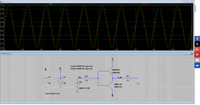
The operational amplifier is inverting the input and with some gain and using push-pull BJT booster stage can have 0 to -3.3 V across the load. I have simulated the attached circuit using sine wave full swing at the input on the operational amplifier, just to see the output.

I have some questions.
1- It has been mentioned earlier that there has to be a feedback resistor for stability. I am not sure if I am getting it completely. Kindly explain bit more where can I put the feedback resistor.

2- The push-pull class AB stage have cross-over issue which can be resolved by two diodes or biasing the gates of both BJTs in such a way that they always conduct. It's not an issue if we don't solve the cross-over issue completely. We don't need full swing anyways.

3- There also has been mentioned in earlier comments about the gain margin and the phase margin. I need some help here too. Kindly have a look at the attached circuit and let me know how can I address them along with the stability.

4- How clean would be this adjustable negative power supply using operational amplifier and push-pull BJT booster stage, compared to SMPS and linear regulators.
 

Attachments

  • Untitled 744.png
    Untitled 744.png
    63.5 KB · Views: 73
Hi,

I don´t know what to do.
Should I repeat what I have written before, especially post#3?
Do you even read my posts?

Klaus
 
2- The push-pull class AB stage have cross-over issue which can be resolved by two diodes or biasing the gates of both BJTs in such a way that they always conduct. It's not an issue if we don't solve the cross-over issue completely. We don't need full swing anyways.


Huh? Crossover distortion has ABSOLUTELY NOTHING to do with full swing. This is like saying “I’m not concerned about getting eaten by a lion, I’m a vegetarian.”
 
This must be frustrating for you when you do not see the fundamental weaknesses of your suggestions and keep getting criticism.

1. As Klaus said ... Rfb must be on output. The crossover error is attenuated by your huge feedback gain (f).
ACTION: join define specs for risetime or BW=0.35/Tr and signal error amplitude in % or mV.
2. You said don't need full-swing. You must always provide specs on what you need ! You already said Vout = 0 to -3.3 V. We assume this is full-swing. However, Vpk-pk has nothing to do with X-over distortion. It only depends on the load current changing push-pull directions.
3. The common emitters are poor driver choices as the collector current source is high impedance and sensitive to pF load phase shift. (OK? high RC) The emitter follower reduces output impedance by source/hFE. (Get it? low RC) This is a much better choice. You won't lose much phase margin as a result. The gain is important to know at the BW you specify as this attenuates the crossover error. The other critical factor is don't forget Ic/Ib = 10 near low Vce so adjust Rb = 60 is required if Load = 3V/0.5A=6 ohms. But Ro on the Op Amp is already higher than 60 so the choice of the PNP is critical for high hFE, and rated for a current much higher than the load like 3A and large enough to dissipate 1W/40'C. It is hard to find a power transistor with hFE> 300 so your true load specs are critical.
4. I think Vee=~ -4V is better for Vout=-4+Vbe = -3.3 for minimum heat rise from Vce*Ic * Rja ['C/W].

ACTION: joni to confirm/ list ALL Specs, incl. load and Vee so choices on active BJT's and Rb are adequate. A heat sink may/will be necessary.
 
Last edited:
The input to the OpAmp is 0 to 3.3 V. I am using OpAmp in unity gain inverting configuration. The output of the OpAmp will be 0 to -3.3 V. The problem is that the output current of the OpAmp I have selected can not deliver 500 mA
Something like this?

1719036943402.png
 
I simulate with full swing. But in actual we will not work with full swing.

I can add two match diodes or proper biasing using resistors at the base of both BJTs to remove the requirement of Vbe more than 0.6 V or 0.7 V to turn them on. This is to address cross over.

The circuit shown in post #17 seems to work as well.

I will read again post #3 and also post #16.

Addressing Post #3:
"Some phrasing corrections:" Yes I agree that the input to operational amplifiers Vin+ and Vin- is close to zero. The unity gain is Gain = 1. The name of the operational amplifier is AD8397. There was a mistake in my original post.

Addressing Post #3:
"To the schematic:" The input capacitors and the output de-coupling capacitors are missing. I need to add them. The positive voltage supplies in the schematic should be placed on top and the lower voltages on the bottom of the schematic. This is known and will be taken care next time. The operational amplifier AD8397 is dual. The other operational amplifier will not be floating.
 
Last edited:
Hi,
I will read again post #3 and also post #16.
I try to write important things first. (does not always work)
thus the first three lines are the more important...

I asked what do you want to be the your output node. ... because
* one the one hand one may expect the bjt output as output
* but on the other hand you labeled the OPAMP output as V_out
(no reaction from your side)

Then I asked you to connect the feedback to the node you want to regulate.
(no reaction from your side)
Basically what Crutschow in post#17 did. And it seems to work.

***

You fucussed and the less important items at the end of the post..
They are good to know ... make things easier for us to read your schematics ... but they wont solve the accuracy problem.

Klaus
 
Last edited:
Coincidentally I see Crutchow had a similar idea to removing NPN, this morning, as I did.

But there are more details to examine.

- Heat dissipation for small SMT packages, input capacitance & unity gain are problems.
- Shared drivers with high fwd Beta and R balancing are solutions.

- The IC datasheet specifies the output current drive is poor at unity gain Rail to Rail and suggests |Av| >=2. So I used that.

A dozen other design details are added to the schematic.
This shows the design can be pushed 6x the required current more Pd can be dissipated by sharing using a test with 1 Ohm load.

1719066401973.png


Previous failed attempts to show progressive improvements. Previous examples had resistors reverse with inverted currents shown for emitter followers. It also had gain and offset errors due to Cin of U1 causing lower Zin (f) and higher voltage drop from
Vdrop=Rs*Cin*dVin/dt

1719066456179.png

--- Updated ---

Added LTspice file.
 

Attachments

  • 1719066370916.png
    1719066370916.png
    293 KB · Views: 56
  • push-pull AD8397.zip
    1,012 bytes · Views: 43

LaTeX Commands Quick-Menu:

Part and Inventory Search

Welcome to EDABoard.com

Sponsor

Back
Top