Continue to Site

Welcome to EDAboard.com

Welcome to our site! EDAboard.com is an international Electronics Discussion Forum focused on EDA software, circuits, schematics, books, theory, papers, asic, pld, 8051, DSP, Network, RF, Analog Design, PCB, Service Manuals... and a whole lot more! To participate you need to register. Registration is free. Click here to register now.

Coss related switching losses (Eoss)

Status
Not open for further replies.

CataM

Advanced Member level 4
Joined
Dec 23, 2015
Messages
1,275
Helped
314
Reputation
628
Reaction score
312
Trophy points
83
Location
Madrid, Spain
Visit site
Activity points
8,409
Hello everyone,

I saw this Infineon advertising product video:
https://www.infineon.com/cms/media/eLearning/PMM/eLearning_600VCoolMOSCFD7/

In the section "Technical features and benefits" --> "Improved switching losses Eoss II", at the end of the video they show how they calculate switching losses. They add to the "Eon" energy (based on drain-source voltage overlap with drain current) the "Eoss" one. Infineon and some other well known manufacturers do this, while others stop at the overlap between drain voltage and drain current in order to estimate switching loss.
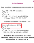
Eoss.png

P.S: They say "Eon" is negligible for 25V, so they account only for "Eoss" in the CFD7 example.

I believe adding "Eoss" to the whole "Eswitching" is mistaken, but since so many others include it, makes me back up..

The explanation why Eoss should not be included in the overall switching loss is this (please tell me if I am mistaken):
Notation: "Id" is the current flowing into the drain of the MOSFET and NOT into the channel. In other words, "Id"=channel current + current into the parasitic capacitors i.e. the current one can measure.

-During turn ON, the Coss capacitor discharges into the channel of the transistor, making the current into the channel of the transistor be higher than the one we are measuring, i.e., channel current=Id (measured with scope) + additional current from the Coss discharge. Hence, using the Vds*Id|during switch ON time makes us underestimate the turn ON switching loss because the "Id" current we are measuring is less than the actual current flowing into the channel of the transistor. The actual switching loss during switch ON needs to have the loss of the Coss.

-During turn OFF, throughout the drain-source voltage switching instance, when we assume the drain current stays constant, the Coss capacitor is being charged with current from the channel of the transistor, so, in the channel of the transistor actually flows less current than the one we are assuming (i.e. measuring at the drain terminal). So, using the Vds*Id|during switch OFF time makes an overestimation of the turn OFF switching loss.

-Combining turn ON loss (underestimation) and turn OFF (overestimation), due to the energy conservation i.e. the energy Coss bleeds out, the same must be replaced, Eoss is nulled into the whole switching process.
In other words, I am claiming this:
turn ON loss --> Vds*Id|during switch ON time + Eoss
turn OFF loss --> Vds*Id|during switch OFF time - Eoss
Overall switching loss --> Vds*Id|during switch ON time + Vds*Id|during switch OFF time

Am I overlooking something ?
Any comment is appreciated !
 

The turn OFF snubber works the same as the Coss during the turn OFF. The turn OFF snubber is widely used for that purpose, but surprisingly, major manufacturers do not account Coss during turn OFF, only during turn ON.
I think the worst case scenario does not apply in this case because it simply is a misconception if accounting Eoss during turn ON but not subtracting it during turn OFF.

turnOFFsnubber.png

During turn OFF, iQ=IL-iC, leaving lower current for the transistor. This is the same Coss does, the only difference is that we can not measure it nor can see the Coss physically.
I do not understand why manufacturers use the turn OFF snubber but they do not apply the same thing for the Coss.
 

Don't forget there will be a voltage overshoot, on the xtor, for the diode catch snubber, due to the L inherent in the load and the Csnub.

- - - Updated - - -

Coss (true) is quite small and reduces as the volts rise unless you are switching at > 300kHz, you can largely ignore it as far as turn off losses go - for highish volts on the drain you cannot ignore it for turn on losses ...

- - - Updated - - -

Say Coss is 1nF and you are turning off 20A i/c = dv/dt, the drain will reach 400V say in 40nS, for an average 10A (half of the 20A) the small amount of power that goes into Coss every 40nS rather than dissipated in the xtor can be largely ignored except at very high switching freqs
 

Say Coss is 1nF and you are turning off 20A i/c = dv/dt, the drain will reach 400V say in 40nS, for an average 10A (half of the 20A) the small amount of power that goes into Coss every 40nS rather than dissipated in the xtor can be largely ignored except at very high switching freqs
I do not get this. If some amount of energy when the xtor turns OFF goes into Coss, then the same amount when the xtor turns ON will go into the xtor, giving a null net balance of energy lost in the xtor due to Coss. The energy does not care about the frequency.
 

-During turn OFF, throughout the drain-source voltage switching instance, when we assume the drain current stays constant, the Coss capacitor is being charged with current from the channel of the transistor
I think this is where you're tripping up. No, the charge/energy in Coss does not come from the FET. It ultimately comes from your Vin or Vout, and some of that energy is lost when the FET turns on. FETs cannot source energy (at least at steady state), they can only dissipate it.

Hard switching a capacitor using switches is always a lossy process, even if the switch resistance approaches zero. This is also why gate drivers require average power, even though their loads are ideally just capacitors. Each switching cycle the energy stored in the capacitance must be wasted, it can't be returned to the source (unless you're using a fancy resonant circuit).
 
Last edited:

No, the charge/energy in Coss does not come from the FET. It ultimately comes from your Vin or Vout, and some of that energy is lost when the FET turns on. FETs cannot source energy (at least at steady state), they can only dissipate it.
I also thought the same thing as you at the beginning, saying that Vin actually supplies the load current + additional current to charge Coss. This is incorrect. Please note from post #2 that the inductive clamped test (idealized) is realized with ideal DC current source, in other words, the current taken from the DC voltage source is a DC constant current i.e. the voltage source can not supply additional current for the charge of Coss.

I agree that I have explained it wrong though.
I said: "[...] the Coss capacitor is being charged with current from the channel of the transistor" <--- confusing sentence, but the ultimate conclusion is the same.
Should have said: "since the current flowing into the drain is constant because we are using a DC current source - see post #2 circuit (forget about the snubber), some current from the DC current source is diverted from the channel and is sent to charge Coss. In other words, Idrain (the current we have access to measure in a real circuit, that is, the channel current can not be measured in a real circuit)=IL(note that it is a DC current source i.e. its value can not change)=Ichannel+Icharge Coss".

Now, one would say: Well, you are using a DC current source, so the current is constant. In a real circuit there would be an inductor and you may say that the supply actually increases the current of the inductor just to charge Coss... I do not see that as a plausible explanation. I think we can agree that the inductor during turn OFF acts as a constant current source.

- - - Updated - - -

Also please notice that the turn-OFF snubber would not make sense if I am mistaken. Why would someone add a capacitor in parallel with a transistor and call it "turn-OFF snubber" if actually it does not help in the turn OFF loss. If the supply would have increased the current of the inductor (load) just to charge the additional capacitor, we would have been in the same thing. MOSFET with the same loss + additional loss due to the supply increasing current to charge the "turn OFF snubber". IT DOES NOT MAKE SENSE !

The turn-OFF snubber cap diverts some current provided by the load into the snubber cap, reducing the current into the drain of the transistor and hence lowering the switching loss during turn OFF. The snubber cap is doing the same thing Coss does !
 

When the fet turns off, Coss absorbs some (a very little) energy from the thing driving current into the device, Coss is non linear with rising voltage so the exact energy can only be roughly computed.

In no way does this reduce energy dissipated by the fet - excepting that if Coss was larger and you turn the fet off in 10nS say, then the turn off losses in the fet channel are smaller - as current at low voltage is diverted to the capacitance - this is a principle of ZVS resonant converters - which have low turn off losses. These often has caps across D-S to exploit this effect.

At turn on the loss in the fet is 0.5 C V^2 f where C = Ceffective. as the freq goes up so does the dissipation, a more major contributor is the reverse recovery of the diode in the other leg (if there is one).

However you cannot balance the two effects and say there is nil effective net loss, there is always turn on loss for higher volts on the drain, but yo can minimise turn off loss - and in a ZVS converter you can reduce turn on loss to near zero as the fet is already on and conducting in reverse when the gate signal is applied.
 

I also thought the same thing as you at the beginning, saying that Vin actually supplies the load current + additional current to charge Coss. This is incorrect. Please note from post #2 that the inductive clamped test (idealized) is realized with ideal DC current source, in other words, the current taken from the DC voltage source is a DC constant current i.e. the voltage source can not supply additional current for the charge of Coss.

I agree that I have explained it wrong though.
I said: "[...] the Coss capacitor is being charged with current from the channel of the transistor" <--- confusing sentence, but the ultimate conclusion is the same.
Should have said: "since the current flowing into the drain is constant because we are using a DC current source - see post #2 circuit (forget about the snubber), some current from the DC current source is diverted from the channel and is sent to charge Coss. In other words, Idrain (the current we have access to measure in a real circuit, that is, the channel current can not be measured in a real circuit)=IL(note that it is a DC current source i.e. its value can not change)=Ichannel+Icharge Coss".
I sort of see where you're going with this, but the difference you're elaborating is irrelevant. Lets go with your revised statement (during turn off, Idrain is divided among the channel and Coss). This means that some energy is stored in Coss. For a hard switching circuit, this energy is always dissipated in the FET during turn on. That energy originally came from Vin (there's no other source in the system). If Coss had not been there, then that energy would have been diverted elsewhere (the load, probably).
Also please notice that the turn-OFF snubber would not make sense if I am mistaken. Why would someone add a capacitor in parallel with a transistor and call it "turn-OFF snubber" if actually it does not help in the turn OFF loss.
That particular snubber works by limiting the rise time of Vds such that dissipation in the FET due to overlap in Vds and Ids is reduced. The energy absorbed by the snubber cap is still dissipated, but in the snubber resistor. So it reduces FET dissipation, but overall circuit dissipation won't decrease.
 

However you cannot balance the two effects and say there is nil effective net loss
I did not say that there is zero turn ON loss. Review post #1. Only the net "Eoss" loss nulls out in the whole switching process which includes both turn ON and turn OFF. There is still loss due to overlap between drain voltage and drain current.

Coss absorbs some (a very little) energy from the thing driving current into the device, Coss is non linear with rising voltage so the exact energy can only be roughly computed.
I think Co(er) characterizes the energy associated with Coss and could give more than a rough estimation...

This means that some energy is stored in Coss. For a hard switching circuit, this energy is always dissipated in the FET during turn on.
Agreed. YOU SAID IT ! At turn OFF, some energy is stored into Coss. At turn ON, the SAME energy is dissipated into the FET.
Where does that energy come from ? It comes from the source, so, Source energy = Energy lost in FET during turn OFF switching + Energy to the Coss.
At turn ON: Source energy = Energy lost in FET during turn ON - Energy that comes back from the Coss
So, does not make this Coss-related-energy irrelevant to the overall(turn ON + turn OFF) switching loss of the FET ?

Please note, that the current taken from the source during turn OFF is constant, because we assume the inductor behaves like a constant DC current source. So, since the current is constant, IL=Ichannel+Icharge Coss => Ichannel=IL-Icharge Coss which is less than IL !
This is the same as saying: turn OFF loss --> Vds*Id|during switch OFF time - Eoss (here Id=IL i.e. drain current and not channel current).

The energy absorbed by the snubber cap is still dissipated, but in the snubber resistor. So it reduces FET dissipation, but overall circuit dissipation won't decrease.
Agreed. The Coss does the same thing, with the difference that its energy goes back to the FET. So, the energy taken out from the FET during turn OFF is dissipated back into the FET during turn ON !
Can you see that Coss does the same thing as the snubber, with the only difference being that the Coss returns the energy back to the FET ?

- - - Updated - - -

That particular snubber works by limiting the rise time of Vds such that dissipation in the FET due to overlap in Vds and Ids is reduced.
I agree that the snubber limits the rise time of Vds, but that is a drawback because more time there is overlap => more power loss. The real reason it reduces the power loss is because it reduces the channel current via diverting some of it into the snubber cap, and then dissipate it into the resistor (don't get me wrong. It does not take energy from the channel, but the current flowing into the transistor is lower because we have added a node, and using KCL says it must be the sum. LOAD current=Drain Current+Snubber Current). The Coss does the same thing with the exception that instead of dissipate it into the resistor, it dissipates it into the FET again i.e. it returns the previously energy stored back to the FET.
 

Far more energy than that contained in Coss can be absorbed by the fet channel at turn on - depending on how fast you turn it on...!
 

Agreed. YOU SAID IT ! At turn OFF, some energy is stored into Coss. At turn ON, the SAME energy is dissipated into the FET.
Where does that energy come from ? It comes from the source, so, Source energy = Energy lost in FET during turn OFF switching + Energy to the Coss.
Ok.
At turn ON: Source energy = Energy lost in FET during turn ON - Energy that comes back from the Coss
No. That energy does not go back to the source.
So, does not make this Coss-related-energy irrelevant to the overall(turn ON + turn OFF) switching loss of the FET ?
No, because that dissipation depends on Coss.

Please note, that the current taken from the source during turn OFF is constant, because we assume the inductor behaves like a constant DC current source. So, since the current is constant, IL=Ichannel+Icharge Coss => Ichannel=IL-Icharge Coss which is less than IL !
This is the same as saying: turn OFF loss --> Vds*Id|during switch OFF time - Eoss (here Id=IL i.e. drain current and not channel current).


Agreed. The Coss does the same thing, with the difference that its energy goes back to the FET. So, the energy taken out from the FET during turn OFF is dissipated back into the FET during turn ON !
Energy cannot come our of the FET (its channel, that is). A channel cannot be an energy source.

I agree that the snubber limits the rise time of Vds, but that is a drawback because more time there is overlap => more power loss.
Longer overlap means more dissipation in the case that both Ids and Vds are being slowed down in the same way. If you slow down the rise of Vds while keeping the drop of Ids fast, then dissipation decreases. However if I also slow down the falling Vds edge while keeping the rising Ids fast, that will increase dissipation. That's why this circuit is built to only slow down the rising Vds edge.
 

For plain hard switching you are unlikely to add a cap across a fet - due to increased turn on losses ( and the current spike at turn on..!) even though you will reduce turn off losses for a fast solid gate drive.

However for a resonant ZVS ckt - capacitance is routinely added to give lower turn off losses - agressive turn off gate drive has the channel off before Vds rises more than 10-20V.

For hard switching more elaborate means are needed to isolate a turn off snubber cap from the fet (a diode - a very good diode) and then re-cycle that energy to the local HVDC bus before the next turn off. Turning a fet on fast can reduce turn on losses - except where you are commutating a non SiC diode - and the very high dv/dt on the fet drain is a nightmare for RFI induced interference ( to your control) and for EMC compliance ...
 

No. That energy does not go back to the source.
Since the source energy is constant during that instant and the MOSFET energy is higher due to Coss discharge into it, in order to keep it constant, you must subtract the Coss energy. It does not go back to the source, source energy stays constant. Actually if you rearrange terms, you see that the energy goes into the FET.

Energy cannot come our of the FET (its channel, that is). A channel cannot be an energy source.
It does not take energy from the channel i.e. the channel is not an energy source, but the current flowing into the channel is lower because we have a node, and using KCL it must be the sum. LOAD current=Channel current+Coss current.

Do you agree with this equation? During Miller plateau of turn OFF : IL=Ichannel + ICoss ? (assume circuit of post #2 without snubber)
Do you agree that "IL" is constant and its value can not change ?
Do you agree that if "IL" is constant and its value can not change, the same is the current flowing through the voltage source during the Miller Plateau of turn OFF ?

The thing I do not agree with you is that you think that during turn OFF the source supplies additional energy to charge Coss. That is impossible because the current through the voltage source is constant and can not change !
Longer overlap means more dissipation in the case that both Ids and Vds are being slowed down in the same way. If you slow down the rise of Vds while keeping the drop of Ids fast, then dissipation decreases. However if I also slow down the falling Vds edge while keeping the rising Ids fast, that will increase dissipation. That's why this circuit is built to only slow down the rising Vds edge.
In a clamp inductive switching, while the voltage rises, the current stays constant and vice versa. So, if you longer the time of rise of the voltage, you can counteract that via lowering the current at which the drain stays constant at => this is done by introducing an additional cap in parallel during turn OFF which "stoles" (or better said, is being diverted some current from the load to it leaving less current for the transistor to switch) - the turn OFF snubber already presented.
I agree though that using the snubber there is an improvement in the drop time of the drain current due to reduced Plateau voltage due to reduced drain current.
 

Since the source energy is constant during that instant and the MOSFET energy is higher due to Coss discharge into it, in order to keep it constant, you must subtract the Coss energy. It does not go back to the source, source energy stays constant. Actually if you rearrange terms, you see that the energy goes into the FET.
This literally doesn't make physical sense. Voltage/current sources do not have "energy" defined at any instant.


It does not take energy from the channel i.e. the channel is not an energy source, but the current flowing into the channel is lower because we have a node, and using KCL it must be the sum. LOAD current=Channel current+Coss current.

Do you agree with this equation? During Miller plateau of turn OFF : IL=Ichannel + ICoss ? (assume circuit of post #2 without snubber)
Do you agree that "IL" is constant and its value can not change ?
Do you agree that if "IL" is constant and its value can not change, the same is the current flowing through the voltage source during the Miller Plateau of turn OFF ?
Sure for your hypothetical circuit these are all true. None of this addresses energy or power though.

The thing I do not agree with you is that you think that during turn OFF the source supplies additional energy to charge Coss. That is impossible because the current through the voltage source is constant and can not change !
Constant current does not mean constant power or constant energy per cycle. Show your work.
 

This literally doesn't make physical sense. Voltage/current sources do not have "energy" defined at any instant.
I was not meant at any instant. I meant throught the whole plateau region. E=V*I*time it takes the plateau

Sure for your hypothetical circuit these are all true. None of this addresses energy or power though.
No, but it is easy to derive them. I was addressing the current because it is where the misconception lies. Once you know the expression for the current, it is straight forward to derive the energy...
Constant current does not mean constant power or constant energy per cycle. Show your work.
I never said "per cycle". The only thing I was referring so far was in the Miller Plateau region, which is where current is "stolen" from the source, leaving less for the channel because it is there where dv/dt happens and hence current into the Coss cap is inserted.

O.K. Here is the derivation.

Here are the waveforms of the clamped inductive load switching (post #2 circuit without snubber) during turn OFF, just to have a common notation of times.That Miller Plateau region happens from "t1" to "t2":
TurnOFF.png

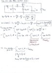
The derivation is attached as a PDF file as well, for better viewing.
TurnOFF-MillerPlateau.jpg

As you can see, because the channel current is smaller, when we measure the actual load current (IL) and use the usual overlap formula, we actually need to subtract the Eoss because some of the current is diverted to the Coss to charge it. At turn ON happens the exact opposite. At turn ON you need to actually sum the Eoss to the usual overlap loss.

- - - Updated - - -

For plain hard switching you are unlikely to add a cap across a fet - due to increased turn on losses ( and the current spike at turn on..!) even though you will reduce turn off losses for a fast solid gate drive.
In hard switching, do you estimate the switching loss due to both overlap as well as Eoss ?
 

Attachments

  • Turn OFF-Miller Plateau.pdf
    260.8 KB · Views: 182
Last edited:

I follow you find up until the last integral in your pdf. You don't take into account that Vds(t) will be dependent on the value of Coss, and therefore so will that integral. Same for the turn on.

Just to clarify, are you claiming that losses due to Coss should be lumped into the Eon and Eoff specified in datasheets? Or are you claiming that Coss doesn't actually play a part in switching losses?
 

I follow you find up until the last integral in your pdf. You don't take into account that Vds(t) will be dependent on the value of Coss, and therefore so will that integral. Same for the turn on.
I should have pointed out clearly (which I did not) that Coss is dependant on Vds, so in all places where you see Coss, actually should be Coss(Vds) showing that Coss is a function of Vds. But I did not in order not to confuse it with Coss multiplied by Vds..
The last integral Eoss@Vbus is actually Eoss@Vbus=1/2 * Co(er)*Vbus^2 (i.e. it is not Coss, but it is Co(er) for the specified bus voltage). That is why I jumped from the integral into Eoss, which would be taken from the datasheet.

are you claiming that losses due to Coss should be lumped into the Eon and Eoff specified in datasheets? Or are you claiming that Coss doesn't actually play a part in switching losses?
The second one i.e. Coss doesn't actually play part in switching losses (it plays part in both turn ON and turn OFF, but it is nulled out in a switching period). Why? As you can see, during turn OFF, if we compute switching loss due to overlap, it is: Vbus*IL|for the time period switching occurs - Eoss (we need to subtract Eoss).

During turn ON, switching loss due to overlap is exactly opposite: Vbus*IL|for the time period switching occurs + Eoss (we need to add Eoss).
If you add Eoss and then subtract it, in a switching period (that is, turn ON + turn OFF switching losses), Eoss is nulled out. This is what I am claiming (and claimed from the beginning-post #1).
 
Last edited:

I should have pointed out clearly (which I did not) that Coss is dependant on Vds
That's also true, but besides my point, which is that Vds(t) will depend on Coss, and therefore so will the last integral (which you refer to as overlap). The way you wrote it is pretty nice, since it cleanly divides it between energy dissipated in the channel (the left hand integral) and energy stored in Coss (Eoss(Vbus) on the right side. But both of those are going to be functions of Coss to some extent. But this nitpick is actually beside the point...


The second one i.e. Coss doesn't actually play part in switching losses (it plays part in both turn ON and turn OFF, but it is nulled out in a switching period).
Nope.

Let's try a hypothetical. If we were to gradually add more capacitance to Coss, the energy it stores per cycle would increase, and thus Eon of the FET would also increase by the same amount. You're claiming that Eoff will also decrease by the same amount, leading to Eon+Eoff being independent of Coss. Lets say that initially Eon=2uJ and Eoff=1uJ. Now let's say that I add enough capacitance that Eon increases by 2uJ (say Vbus=50V and I add 1.6nF to Coss). Now Eon=4uJ, and Eoff should be.... -1uJ? Do you see a problem with this scenario?
 

Let's try a hypothetical. If we were to gradually add more capacitance to Coss, the energy it stores per cycle would increase, and thus Eon of the FET would also increase by the same amount. You're claiming that Eoff will also decrease by the same amount, leading to Eon+Eoff being independent of Coss. Lets say that initially Eon=2uJ and Eoff=1uJ. Now let's say that I add enough capacitance that Eon increases by 2uJ (say Vbus=50V and I add 1.6nF to Coss). Now Eon=4uJ, and Eoff should be.... -1uJ? Do you see a problem with this scenario?
I see what you are saying, but it is mistaken.
If you rearrange the second equation I have highlighted by placing it into the box in the pdf, you have this: IL=ichannel(t)+Coss(Vds)*dVds/dt.
If you increase Coss, the equation must hold, so dVds/dt decreases. You can see that this is the reason the turn OFF snubber (which adds a capacitor in parallel with Coss during turn OFF) makes the transition longer i.e. increases the time, respectively decreases dVds/dt.

ichannel(t) can not go nevative, so the boundary of that equation is IL=0+Coss(Vds)*dVds/dt i.e. up to the point where all the current is diverted to the capacitances Coss and any other in parallel you add (e.g. a turn OFF snubber "Cs").
So, the case you are saying that Eoff<0 is impossible because simply "ichannel(t)" clamps at 0 Amps i.e. there is no channel current because all the current is diverted into the capacitances.

If you look sharp, you can see that this makes sense since increasing Coss (e.g. via adding an additional cap like a turn OFF snubber) => reduces channel current => reduces Vgp (gate plateau voltage) => reduces dVds/dt respectively increases the time it takes for the voltage to rise from 0 to the BUS voltage.

Diverting all the channel current into the parallel capacitors i.e. effectively making ichannel(t)=0 (can not go negative) is effectively shutting off the transistor and hence clamping "Vgp" to the threshold voltage i.e. Vgp=Vgs(th). In other words, Eoff=0, NOT negative.

If you increase the parallel capacitance even further i.e. to the point ichannel(t) would have gone negative, the ichannel(t) does NOT go negative but simply the equivalent circuit I have drawn is redrawn making ichannel(t)=0 and leading to the equation: IL=(Coss+Any additional Cap)*dVds/dt.
As you can see, once you pass the boundary condition (i.e. you add too much capacitance), since IL is constant => Coss is increased from Coss to Coss+Additiona cap i.e. => dVds/dt is decreased which is a drawback !
Furthermore, if you do not give that alternative path like a turn OFF snubber does, that energy you put into the cap, it gets back to you at turn ON. So you would have Eoff=0, but Eon rises a lot more because you are overcharging more than necessary that additional cap you add in parallel unless you give that energy an alternative way to go, like the turn OFF snubber does, discharging the energy into the resistor.

To give you an example. If I were to design a Turn OFF snubber or in other words, to add the necessary capacitance in parallel to Coss, I will aim for the boundary condition i.e. do not go further ! That is like this:
  • ichannel(t)=0 => IL=(Coss+Cadditional)*dVds/dt (1)
  • Vgp=Vgs(th) because we are at the boundary => Cgd*dVds/dt=Vgp/Rg <=> dVds/dt=Vgs(th)/(Cgd*Rg) (2)
  • Insert (2) into (1) and compute Cadditional. This theory looks good but Cgd is highly nonlinear. So, we need to find dVds/dt in another way, using gate charge, like this: Ig=Vgp/Rg => trise of voltage=Qgd@Vbus*Rg/(Vgp) => dVds/dt = Vbus/trise of voltage
  • The other problem is that we still have Coss in (1)... that can be solved by using Co(tr)... I think

The thing that bothers me most, is that manufacturers use Eoss at turn ON, but they do not say how Eoss was placed into Coss in the first place. Didn't some energy go into the Coss to give birth to that Eoss in the first pleace, lowering hence losses into the transistor at turn OFF (even though at turn ON you regain that Eoss losses, but overall Eoss is nulled out) ?

- - - Updated - - -

Looking at (1), since ichannel(t)=0 and can not go negative, dVds/dt will decrease to compensate for the increase of Coss+Cadditional.
So, inserting too much Cadditional has no benefit because it slows down the rise of the voltage.
 
Last edited:

I agree with pretty much everything in that post, which is strange because you previously said this:
The second one i.e. Coss doesn't actually play part in switching losses (it plays part in both turn ON and turn OFF, but it is nulled out in a switching period).
Which can't be true since, as you just pointed out, Eoff can't be negative, but Eon can grow indefinitely.

The thing that bothers me most, is that manufacturers use Eoss at turn ON, but they do not say how Eoss was placed into Coss in the first place. Didn't some energy go into the Coss to give birth to that Eoss in the first pleace, lowering hence losses into the transistor at turn OFF
I think the logic is that they associate Eoss with Eon because that's when Eoss is actually dissipated by the transistor, as opposed to simply being absorbed by the transistor (along with its Coss). For most purposes the total Eon+Eoff is what counts, so it hardly matters. But my point is still that (Eon+Eoff) may depend on Coss, so Eoss can't be ignored entirely.
 

Status
Not open for further replies.

Similar threads

Part and Inventory Search

Welcome to EDABoard.com

Sponsor

Back
Top