Continue to Site

Welcome to EDAboard.com

Welcome to our site! EDAboard.com is an international Electronics Discussion Forum focused on EDA software, circuits, schematics, books, theory, papers, asic, pld, 8051, DSP, Network, RF, Analog Design, PCB, Service Manuals... and a whole lot more! To participate you need to register. Registration is free. Click here to register now.

[Moved]: Ultra-low Power Bandgap Reference design

Status
Not open for further replies.

zilch

Member level 2
Member level 2
Joined
Sep 9, 2014
Messages
48
Helped
1
Reputation
2
Reaction score
1
Trophy points
8
Activity points
323
Good day!

I am currently designing an ultra-low power bandgap reference in 65nm CMOS technology that is supposed to produce reference voltage of at least 200mV. The supply voltage that we initially planned was from the output voltage of a rectifier which is very small. But for now I am using a 0.45V as a supply voltage ( i just assumed that our rectifier will have an output of around 0.45V since we divided the work). But i have doubts regarding my design. Should the transistors operate in saturation region?( my MOS are in cutoff at the moment)
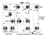
Screenshot_4.png

this topology is from https://ieeexplore.ieee.org/xpl/freeabs_all.jsp?arnumber=7217038&abstractAccess=no&userType=inst

I am still thinking of another question haha
 

Re: Ultra-low Power Bandgap Reference design

... Should the transistors operate in saturation region?( my MOS are in cutoff at the moment)

Of course! What a question :roll:
 

Re: Ultra-low Power Bandgap Reference design

Correct me if I am wrong, but the current reference stage looks like a beta multiplier to me(constant transconductance biasing circuit).

One thing that you could try that has worked for me in the past is to remove the gate to drain connection of M8. Then connect the output of an op-amp to the gate of M7-M8 and tie the positive node of the op-amp to the drain of M3, the negative node to the gate of M1-M3. If area is not a concern, using a resistor instead of a diode connected MOSFET for M2 might give you better voltage headroom, especially with a supply voltage of 0.45V(is this a superthreshold design or are your devices low VT?). Lastly, the gate of M9 would not be connected to node A, but the gates of M7-M8.

I have not actually measured the TC of a constant gm circuit...so I wouldn't know if it would be acceptable for your application.


You really need to make sure that all of your devices are saturated if you want the results that you expect. With two diodes in your current reference, I do not really see how you can operate in saturation unless you have a very low VT.

Lastly, notice how the paper states the supply range they used was 0.8v to 3v. If you want to use 0.45V for your rail, check the 4th citation they provided:A 2.6nW,
0.45 V temperature-compensated subthreshold CMOS voltage
Reference
 

Re: Ultra-low Power Bandgap Reference design

Hi, I changed the architecture of the BGR, the one from "A 2.6nW, 0.45 V temperature-compensated subthreshold CMOS voltage Reference". I think I got the output I wanted. But I still have doubts because when I varied the supply voltage (from 0 - 1.2V), my Vref increased a bit. My design works on 0.6V or above. VDD-variation.pngTemperature-variation.png
 

Re: Ultra-low Power Bandgap Reference design

I think you can be very content with the temperature stability, which seems to be <1µV/K or -80ppm voltage change in the interesting temperature range between 20 and 50°C. Depending on the requirements of your application, you might need a pre-regulation for the BGR (which has ≈ ±1.25% voltage variation between 0.8 and 1.2V).
 

What topology are you using now? Post a schematic. The most likely reason is that you do not have a high enough VGS drop across your current mirrors at low VDD. Which implies that the output current source is not in strong inversion and you cannot supply the current you need to the load diode.
 

This is the topology I'm using. It's purely MOSFETs.

Capture.PNG
 

Perform your simulation using the value you want your supply voltage to be at. So you should set it 0.45V. Then determine what the dc operation points are(annotate on schematic). Ensure that your devices have at least 100mV of headroom above the threshold voltage at that point and it should work(It will work even if you do not have 100mV headroom but when you go and do a PVT analysis with Monte Carlo, I guarantee it will not).

What are the sizes of your devices?

Looking at the schematic, if you make M1 wider, you will decrease the voltage drop across it which will also increase your current mirror overdrive voltage due to the diode connected device M5.

If you make M5, M7, M9 longer, the over drive voltage will increase as well since the VGS drop of the diode increases.

Lastly, if a process solution is acceptable, you can probably substitute LVTs(Low Threshold Voltage devices) for your Traditional MOSFETs which would greatly enhance the overdrive voltage.
 
  • Like
Reactions: zilch

    zilch

    Points: 2
    Helpful Answer Positive Rating
I have set my supply voltage to 0.6V. I have also noticed the effects of making M1 wider, and making M5, M7, and M9 longer.

For the start-up ckt, is it necessary that they operate in saturation region? because in my design most of them are cut-off.
 

The second branch in the start up circuit is an inverter and usually only consumes significant power during dynamic switching, I think the purpose of the two diode connected devices is to set the upper rail on the inverter so M3s is not always on.

The first branch senses if there is current flowing. The only devices that should not be off are these two devices. And you should make sure that the output of the inverter is at the correct value.

You will not notice an effect on the bandgap with the startup during a dc simulation, do a transient simulation to see it ramp up and stabilize at the reference voltage.
 

The first branch senses if there is current flowing. The only devices that should not be off are these two devices. And you should make sure that the output of the inverter is at the correct value.

You mean they should be in saturation region?

- - - Updated - - -

Anyway, I planned to use this BGR to a LDO powered by a storage element.
 

I'm not entirely sure if it needs to be in saturation, but for repeatable results I would bias it into saturation, which shouldn't be hard if your other current mirror devices are in saturation, you can always lower the aspect ratio to reduce the current to reduce quiescent power consumption since that branch of the start up is always on.

If you need more info on LDOs a good source is: Analog IC Design with Low-Dropout Regulators by Gabriel A. Rincón-Mora.
 

Ok noted. Thanks for the reference, ill be back again. Haha
 

Which is better, LDO or charge pump?
 

Depends on what your application is. You might be able to get away with a LDO that is simple and it would take up a lot less area compared to a charge pump.

Personally, I would use a LDO because then you don't have to worry about the switching mechanism of the charge pump. I think the reason people typically use charge pumps is to create negative voltage supplies.

How exactly will this LDO/charge pump be used?
 

How exactly will this LDO/charge pump be used?

To serve as a power source for sensors. Basically, we are working on a energy harvesting system.

- - - Updated - - -

Anyway, how do I regulate the output of my BGR? I'm not yet satisfied with the output based on the screenshot I posted. The peak is about 276mV.
 

First thing I would do is attach a unity gain buffer to the output so you are not affecting the reference.

I am a little confused on what you are trying to do, if you are trying to further decrease the output voltage, I think it would make more sense to do so in the bandgap itself. If you are using the bandgap to provide a reference voltage for an error amplifier for another input signal that you want to use for your sensors, I can show you a relatively simple topology that might work for that.


Or are you talking about curvature compensation?


As an aside, a charge pump is doable but it would be noisier than if you had a linear regulator or sorts.
 

If you are using the bandgap to provide a reference voltage for an error amplifier for another input signal that you want to use for your sensors, I can show you a relatively simple topology that might work for that.

This is what we planned to do.
 

should I increase the reference voltage? Since our rectifier has an output of approx 1.2V.
 

I am still having a hard time trying to visualize what you are doing, if you can provide a schematic it would be very helpful.

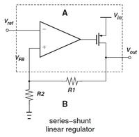
I would not raise the voltage of the bandgap if you are trying to get a voltage that is lower than the bandgap reference. The regulator that I have included below shows a relatively simple topology that will step down the input voltage to the reference voltage of the bandgap plus an additional factor of the resistor ratios.


The output voltage is:

Vout=(1+R2/R1)Vref
 

Status
Not open for further replies.

Part and Inventory Search

Welcome to EDABoard.com

Sponsor

Back
Top