Continue to Site

Welcome to EDAboard.com

Welcome to our site! EDAboard.com is an international Electronics Discussion Forum focused on EDA software, circuits, schematics, books, theory, papers, asic, pld, 8051, DSP, Network, RF, Analog Design, PCB, Service Manuals... and a whole lot more! To participate you need to register. Registration is free. Click here to register now.

[SOLVED] Zero Crossing Detector Circuit Evaluation

Status
Not open for further replies.

d123

Advanced Member level 5
Joined
Jun 7, 2015
Messages
2,505
Helped
494
Reputation
992
Reaction score
525
Trophy points
1,393
Location
Spain
Activity points
27,148
Hi,

Old circuit idea for ZCD, I wanted to see if it could actually be used in the real world (and how to go from sim-world AC generator version to a practical implementation). Would appreciate objective comments on circuit design mistakes, reasons why it couldn't work as desired, and/or things that would be glitchy. Thanks in advance if you have the patience and time.

Block diagram:
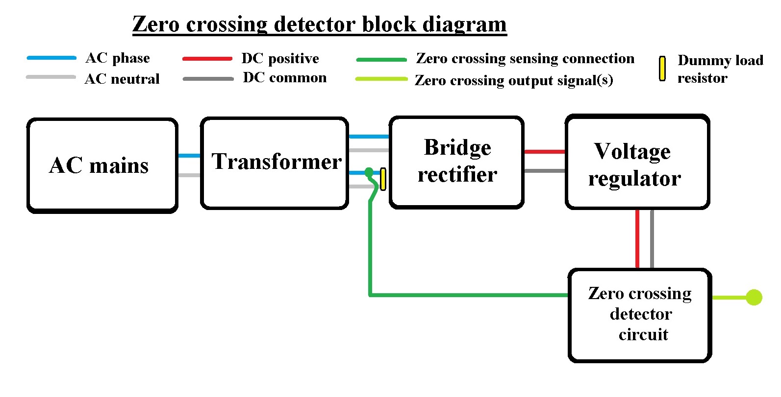
zcd circuit block diagram.jpg


Original idea which has a transient result that (hopefully) shows the purpose of the circuit:
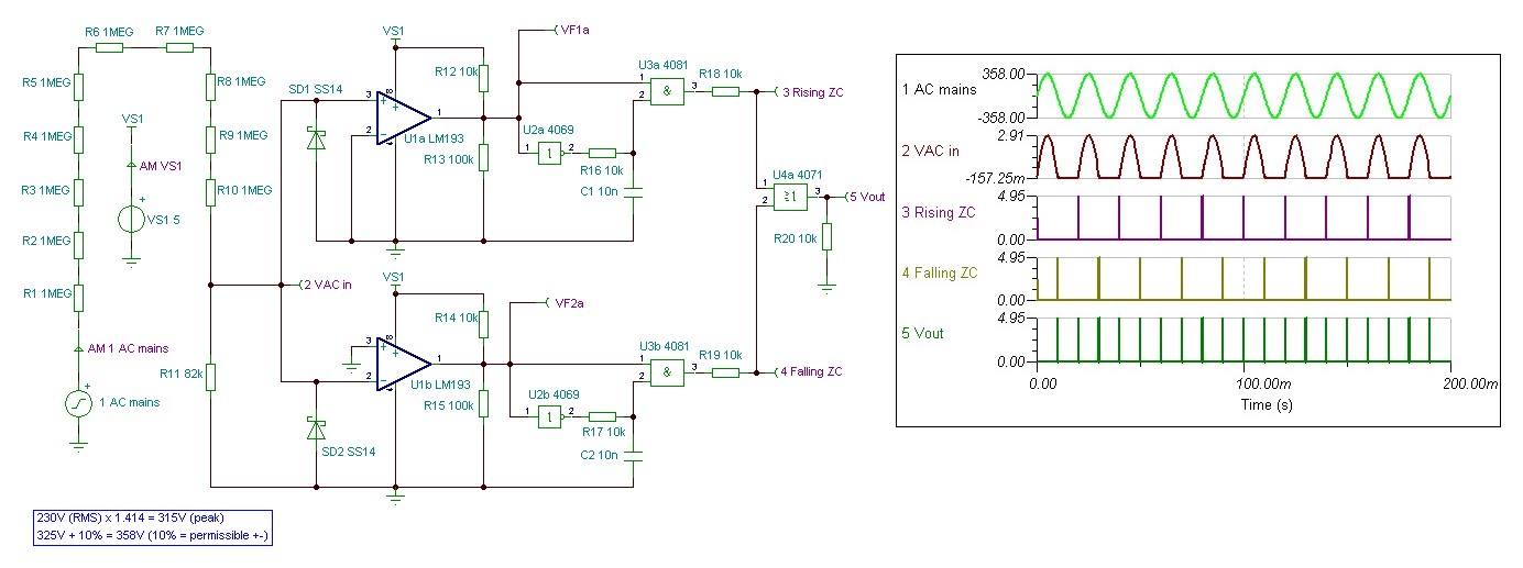
ZCD RISING FALLING BLIP OUTPUT 358VAC PEAK IN.JPG


The version I think could work as a real circuit:
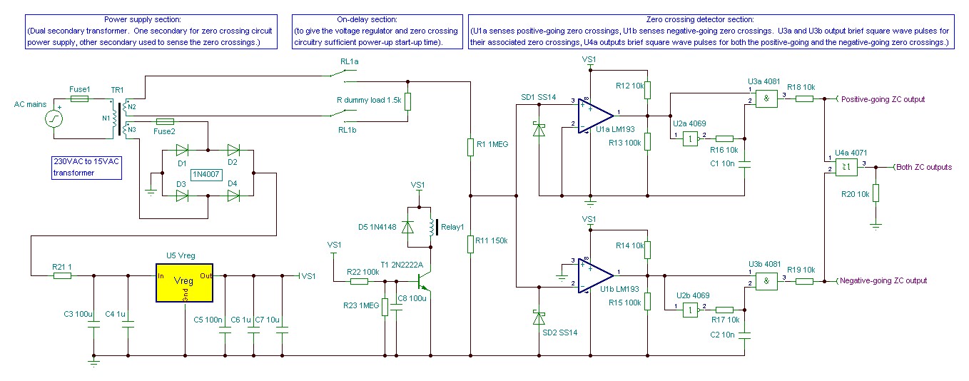
ZCD RISING FALLING BLIP OUTPUT 358VAC PEAK IN WITH TRANSFORMER V3.JPG


Reasons I can think of why it might not work as desired and/or can't/shouldn't be made:

1) I think I'm not allowed to plug a home-made transformer-based power supply into the AC mains unless it includes PFC, even for a circuit that would draw about 60mA.
2) Possibly, this circuit only works correctly (i.e. correctly meaning that the rising square wave pulse always occurs on positive-going and falling pulse always occurs on negative-going zero crossings) if the phase and neutral of the plug socket are known - if the wiring is reversed then the positive pulse would actually be the negative-going zero crossing and vice versa. Is that so?
3) I have read several things today that tell me that the secondary output of a transformer is either 180º out-of-phase with the primary AC sine wave, or that it is only a few degrees out of phase, or that it is never out-of-phase... Which of these is correct?
4) I see that chatter/false zero crossings is very possible from something I read. With regard to 'distorted AC mains', I have no idea how to implement comparator hysteresis for 0V references. Is that the same as for any other hysteresis? Is it really necessary? According to sbaa356, Zero-Crossing Detection with False Trigger Avoidance:
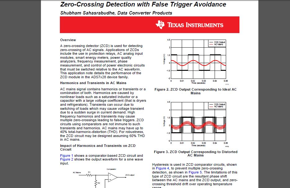

sbaa356 distorted mains false triggering image.JPG


Thanks.
 

1) Who won’t “allow” you to plug a small transformer into the mains? If this is just a hobbyist thing, stop worrying, we’ll visit you in jail. If it’s a product, that’s different.
2) the circuit doesn’t know anything about plug orientation.
, it just knows about voltage.
3) it depends.
4) If you set your hysteresis large enough, you won’t get false triggers.

you could save yourself a chip by using a Schmitt-trigger NAND gate instead of an inverter and AND gate.
 
  • Like
Reactions: d123

    d123

    Points: 2
    Helpful Answer Positive Rating
Hi,

Why it can't work.
TR1_N2 has no relation to your GND, thus ZCD circuit sees no voltage. You need to connect N2 lower side to GND.

I don't understand the relay function. When there is no supply the ZCD won't work. If there is supply the relay will always be ON.

SD1 and SD2 are in parallel. A single diode will do.
But the diode limits negative voltage but does not limit positive voltage. So the signal is non symmetric...take care not to make the ZCD output unsymmetric.

LM193 input voltage range is -0.3V .... can you satisfy this?

The input of both comparators are at same voltage nodes, thus they switch equally...just inverted.
No filter, no hysteresis...this calls for noise pickup.

What do you want to do with the ZCD signal?


Klaus
 
  • Like
Reactions: d123

    d123

    Points: 2
    Helpful Answer Positive Rating
1) Who won’t “allow” you to plug a small transformer into the mains? If this is just a hobbyist thing, stop worrying, we’ll visit you in jail. If it’s a product, that’s different.
2) the circuit doesn’t know anything about plug orientation.
, it just knows about voltage.
3) it depends.
4) If you set your hysteresis large enough, you won’t get false triggers.

you could save yourself a chip by using a Schmitt-trigger NAND gate instead of an inverter and AND gate.

Hi barry,

1) Very funny.
2) Good point...
3) That's not a nice answer - it smells of my having to do lots of reading to understand the ins and outs of the issue.
4) Okay.

That's a good idea about the Schmitt-trigger NAND.

Thanks.
--- Updated ---

Hi,

Why it can't work.
TR1_N2 has no relation to your GND, thus ZCD circuit sees no voltage. You need to connect N2 lower side to GND.

I don't understand the relay function. When there is no supply the ZCD won't work. If there is supply the relay will always be ON.

SD1 and SD2 are in parallel. A single diode will do.
But the diode limits negative voltage but does not limit positive voltage. So the signal is non symmetric...take care not to make the ZCD output unsymmetric.

LM193 input voltage range is -0.3V .... can you satisfy this?

The input of both comparators are at same voltage nodes, thus they switch equally...just inverted.
No filter, no hysteresis...this calls for noise pickup.

What do you want to do with the ZCD signal?


Klaus

Hi Klaus,

Thank you!

I'm terrible with AC signal knowledge/ignorance - I wasn't so sure that was wired correctly, okay.

Relay: The idea is to have no signal going into the comparators until the regulator is regulating and the power supply is functioning correctly, so that the ZCD circuit is ready to accept input signals. The BJT RC on the base introduces a short turn-on delay. Otherwise I would expect runt signals to slip through to the output.

Oh, yes, I hadn't thought about the redundant diode. Sorry, could you please explain what you mean by 'So the signal is non symmetric...take care not to make the ZCD output unsymmetric.' - I do not understand this idea. Positive input will be limited to e.g. 3V, negative input to the Schottky diode Vf.

Only just. The Schottky diodes are supposedly around 0.7 Vf max., but at trivial currents the If vs Vf graph shows something more like 100mV. Assuming they are around 350mV, I can just get away with it, not sure about satisfy LM193 datasheet specifications regarding -0.3V max.

I wanted to avoid adding hysteresis as one of the comparators is the non-inverting configuration and, as far as I remember, that is the one that seems excrutiatingly hard to prevent from becoming unstable no matter what kind of hysteresis is used (in my hands).
Where would a filter go? And, wouldn't adding a filter create further delay between the actual zero crossings and the output signals used to trigger whatever is supposed to turn on as close to the zero crossings as possible?

I have absolutely no idea. Nothing for the time being. It was just a circuit that for the past two years has been like an annoying thought at the back of my mind that I wanted to move from a simulated theory with its unrealistic AC source and excellent transient results to a workable reality at least.
Who knows..., maybe datalog the real frequency of the mains, maybe turn on a power-hungry device like a motor, maybe charge a huge capacitor bank - I don't know what else it would be much use for, those are purposes I understand I would use such a circuit for.
 
Last edited:

In a little more detail:
1. You don't need PFC.
2. Using two comparators to sense small positive or negative voltages around zero is a sensible idea in principle but you first have to establish where that zero actually is. The only practical way to do that is to ground one side of the AC and sense the other side. The polarity will swing positive and negative so your comparators need dual supplies or you have to somehow offset the AC so it always has a positive voltage above zero. You can probably achieve the same accuracy by using a Schottky bridge rectifier (at low current giving you the few hundred mV drop) and a single unipolar comparator.
3. The answer depends on which way the secondary is wired with respect to the primary. Two factors come into play, reversing the secondary will invert the waveform from it so you get an effective 180 degree shift, however, there is also a small phase shift anyway, probably a few degrees, due to the magnetizing and demagnetizing of the transformer core as the current changes direction. The shift is fairly stable so it can often be compensated by delaying the zero crossing output by a fixed amount of time.
4. As you sense smaller and smaller voltages to find the exact zero point, you increase the chances of detecting unwanted signals. AC line power isn't clean as it carries interference from connected devices and to some degree, distortion of the waveform caused by uneven loading elsewhere on the network that might hide the real zero. You can filter much of it out by assuming the only frequency you are interested in in the line frequency but the filter will introduce phase shift of it's own that you need to recognize. Jitter is a slightly different but associated problem, you are dealing with small analog signals and deriving a digital signal (the ZCD) from them. That means there is some threshold voltage which decides the resulting logical state and if the threshold reference and the input signal are not perfectly noise free, the threshold crossing will occur too early or too late. Hysteresis using a Schmitt triggered device helps but at the expense of a wider margin around the zero point.

Brian.
 
  • Like
Reactions: d123

    d123

    Points: 2
    Helpful Answer Positive Rating
Hi,

The idea is to have no signal going into the comparators until the regulator is regulating and the power supply is functioning correctly, so that the ZCD circuit is ready to accept input signals.
Both your comparators switch at around 0V ... consider noise and offset.
Now you switch OFF the input, thus the comparator input is round 0V.
Thus the comparator output is unpredictable. Randomly swithcing, continously ON or continously OFF. Both comaparators independently. I´d avoid this situation.

...Maybe with a RESET circuit, you can suppress the digital ouput of your ZCD circuit.

Positive input will be limited to e.g. 3V, negative input to the Schottky diode Vf.
Yes, this is non symmetric. 3V vs about 0.5V.
I´d try to keep it symmetric. Either both 3V or both 0.5V.
Unsymmetric voltage will lead to unsymmetric timing.

not sure about satisfy LM193 datasheet specifications regarding -0.3V max.
If it´s 0.35V then you´re out of abs. max specification. "Stresses beyond those listed under Absolute Maximum Ratings may cause permanent damage to the device"
Good thing is that the datasheet also specifies a current limit of 50mA. means: it most likely won´t kill the device, ... but datasheet also talks about possible malfunction. Thus - for reliable operation - I´d avoid this situation.

wouldn't adding a filter create further delay between the actual zero crossings and the output signals used to trigger whatever is supposed to turn on as close to the zero crossings as possible?
This is why I asked about the application.
Example:
looking at the RMS voltage difference of a fully ON halfwave comapred to a 175° halfwave is less than 0.01%
(loss of 1% at about 26°)
or in power: 0.016% (loss of 1% at about 20°)

and 5° means: 5° / 180° * 10ms = 0.28ms or 2.8%

In my eyes the ZCD signal needs to be stable (low jitter), but there is no need to extremely go to the real zero cross timing. Also mind: if you try to ignite a triac that close to zero cross it maybe can´t hold for the rest of the halfwave because of too low hold_current. --> it does not ignite at all. (surely depends on ignition method)

your application examples:
* frequency measurement does not need to be exactly at zero cross, but needs to be stable
* motor control: the loss of 0.016% of power won´t harm
* a capacitor bank is charged to it´s peak voltage .. the beginning 5° are not of interest
--> from my experience: don´t worry about a little delay, but worry about jitter, noise...

Klaus
 
  • Like
Reactions: d123

    d123

    Points: 2
    Helpful Answer Positive Rating
Hi,

First, quick picture to explain purpose of NOT gate + RC network into AND gate - with regard to swapping them for a Schmitt-trigger NAND gate. I read a Schmitt-trigger NAND gate datasheet earlier, I haven't understood the timing diagrams but I do understand the truth table and it looks like that what it does is the opposite of what is desired here. Am I misunderstanding the Schmitt-trigger NAND gate operation with regard to this circuit?

NOT RC wrt Schmitt Trigger NAND.jpg


Hi there Brian,

Thank you.

1) Super!
2) I think you mean what Klaus also said about grounding TR1_N2: I have changed that in the schematic. Also, I could use/add a negative supply (TC7660) for the comparators to make the swing symmetrical. Can't envision the Schottky bridge + 1 comparator in my mind yet...
3) I'm gathering this is related to how I wire the secondary with regard to the 'dots'. I don't mind a few or more degrees as 'zero switching' isn't a realistic goal for me and doesn't seem a vital must-have circuit function.
4) Really, I think I need to add an x-order band pass filter somewhere before the inputs set for around 50Hz. (?)

I haven't done anything electronics-related for months and had even forgotten that ground is not some rock-solid 0V but is a bit fluid depending on what's happening elsewhere in a circuit or on return paths...


Hi again Klaus,

Thanks!

Right... better idea about the reset option - funnily enough, I simulated the resistive divider input connected to ground at power-up to emulate the relay idea and the results showed it working correctly, which I found questionable as - as you say - if the inputs are at 0 then surely the comparators would trigger...

With regard to risking abusing the LM193 -0.3V specs with the Schottky diode, and relating to the advice about 'symmetrical', it's just easier to add a negative supply for the comparators with a TC7660, but then I would need to limit the comparators' negative-going swings into the logic gates - so I'm going to think about what is least bad in this case.

This is what I gleaned this weekend from Internet homework reading (except for the thing about Triacs) - 'zero crossing switching' is not a realistic aspiration (without adding additional sections to the circuit or an MCU) and if the point is mainly avoiding turning something on (something that might draw a lot of current) when the AC is at its peak, a few degrees or more past 0º is more than acceptable. I'm under the impression that in this context - in a sense - degrees/voltage/time are almost interchangeable as far as the end result is concerned, if that makes sense.

Jitter, noise - would an x-order band pass be the simplest way of dealing with these issues?
 

Hi,

There are comparators with true logic output (+/- supply but output referenced to GND.)

would an x-order band pass be the simplest way of dealing with these issues?
yes, I´d start with 2nd order.

The more sophisticated solution (I did) is to use a well filtered analog signal then use a PLL to generate more noise free digital signals.

Klaus
 
  • Like
Reactions: d123

    d123

    Points: 2
    Helpful Answer Positive Rating
Hi,

I have tried to implement the suggestions and corrections so kindly provided the other day. In simulations of sub-circuit sections they work great (!). Could someone be so kind as to have a quick look and see if the changes are what was recommended, please? Pictures and brief explanations follow:

With this reduced version, I checked adding a negative supply to the comparators and keeping the comparator Vouts to within CD4xxx inputs acceptable levels (-0.5V), simulation claims less than -200mV using 1N4148s as shown (SS14 Schottkys in their place were very bad, > -500mV). Added minimal hysteresis to 0V references. Added 'on-delay' at outputs.

RESET POR IDEAS 2B NEGATIVE SUPPLY.JPG


For a 50Hz filter, I chose the (inverting output) Deliyannis band pass as the MFB and Sallen-Key band passes were really hard to get to simulate anything I understand I want them to do. As it is inverting, I added an inverting amplifier after it to keep the signal in-phase with the input signal. Is this kind of filter and the results what was suggested I add to the circuit?

DELIYANNIS BAND PASS SLOA096 VERSION.JPG


This is the schematic of the complete circuit with all of the suggested changes (if I've implemented them as intended/correctly is an entirely different matter 😖). I'm unsure if the band pass filter is in the right place, and if additional RC low pass filters are needed at the comparator inputs:

ZCD RISING FALLING BLIP OUTPUT 358VAC PEAK IN WITH TRANSFORMER V5.JPG


Thanks.
 

Hi,

I see many issues - indeed more than before.

* A bandpass in simulation works great. But in reality you have part variations and drift. Both leading to drifting amplitude and drifting phase shift.
--> I see no need for a high pass filter (The transformer does not ouput DC at all). To get rid of distortion you should attenuate overtones. Beginning with 3rd harmonic. Choose a filter that has a relatively flat (horizontal) phase around 50Hz.

* U2 has feedback to inverting input. Thus reducing gain. No hysteresis. But U6 has feedback to noninverting input. Creating high gain and some hysteresis.

* The node of the diode_cathodes is floating ---> no reliable signal.

****
My ideas to simplify things:
* single supply
* create a buffered DC voltage around 2..2.5V (REF1)
* from dummy load: use a series capacitor and a resistive voltage divider R1, R2 ...referenced to REF1
(now at R1 the AC swings around REF1)
* a capacitor across R1 gives the first LPF.
* Use an an inverting OPAMP to Buffer this signal, including the second LPF.
* feed it to a comparator (COMP1), other comparator input to REF1. Add two hystereis resistors.
(comp out now is 50% duty cycle with mains frequency. Switching near zero cross, delayed by the hysteresis)
* feed COMP1 to an RC delay. Feed this to a schmitt trigger (ST1)
* feed COMP1_OUT and ST1_OUT to an exclusive OR.
* use an AND gate to mask the XOR_OUT with the RESET signal.

Maybe just 1/3 of the part count.

Klaus
 
  • Like
Reactions: d123

    d123

    Points: 2
    Helpful Answer Positive Rating
Hi Klaus,

Thanks for taking the time to look at the changes and provide your knowledge. I appreciate it.

Need to look at 3rd harmonic information...

Oh dear... A lot to think about and I'll think further about the version you suggest but I would like to keep at least some of the original circuit...

Thanks
 

Hi,

No problem. It's your design ... and you have to find and go your own way.
Give the same task to 10 engineers and get10 different solutions.

Some thought about your design.

You take much effort in adding several Opamp stages.
In my eyes the stafes U3 and U4 don't bring any benefit.
If U4 can drive the signal, then also U2 will be able.
U3 is just an inverting circuit ... for a symmetrical AC signal .... the comparators won't care...

Klaus
 
  • Like
Reactions: d123

    d123

    Points: 2
    Helpful Answer Positive Rating
You might be well off to use a small xfmr
to sniff the line without letting line into
active circuitry.

Comparator chatter after the zero crossing
event is not necessarily a problem, like the
time I had to do this was just to fire SCRs
in a DC motor drive bridge and it doesn't
matter how many times you poke a SCR's
gate terminal, the first one gets it done.
In timing applications w/ ramp and comparators
I will always use a SRFF to clean up chatter.
A one-shot can be a way to go if you know
how much noise amplitude and duration to
expect.

Is there a reason why you need to get fast
ZC impulses rather than edges? Simpler to just
use a square wave image of line and just get
the ZC-up, ZC-down off those two edges, if
adequately clean (what constitutes adequacy,
the successor circuitry gets to say).
 
  • Like
Reactions: d123

    d123

    Points: 2
    Helpful Answer Positive Rating
H
Hi,

No problem. It's your design ... and you have to find and go your own way.
Give the same task to 10 engineers and get10 different solutions.

Some thought about your design.

You take much effort in adding several Opamp stages.
In my eyes the stafes U3 and U4 don't bring any benefit.
If U4 can drive the signal, then also U2 will be able.
U3 is just an inverting circuit ... for a symmetrical AC signal .... the comparators won't care...

Klaus
Hi Klaus,

Engineers find solutions; hobbyists (like me)..., well, I'll say no more...

Explain it to me in 'stupid', please, because I'm not sure if I'm missing/misunderstanding something... If the band pass filter (U2) inverts the input signal 180º, by my understanding and reasoning I would add an inverting amplifier stage (U3) to invert that inverted signal another 180º to make it the same as/in phase with the input signal. Thus, my 'rising zc' and 'falling zc' are not inverted at their outputs, because if I left the input signal 180º out of phase with the input, the 'rising' would really be the 'falling' zero crossing and vice versa. Is there something wrong with my reasoning about that?

I always have doubts about op amps with feedback and when/if the previous and subsequent stages that may also contain feedback or voltage dividers, etc., will affect their operation, so I shove buffers everywhere, just in case. So U4 is unnecessary, but U1 is necessary?
--- Updated ---

You might be well off to use a small xfmr
to sniff the line without letting line into
active circuitry.

Comparator chatter after the zero crossing
event is not necessarily a problem, like the
time I had to do this was just to fire SCRs
in a DC motor drive bridge and it doesn't
matter how many times you poke a SCR's
gate terminal, the first one gets it done.
In timing applications w/ ramp and comparators
I will always use a SRFF to clean up chatter.
A one-shot can be a way to go if you know
how much noise amplitude and duration to
expect.

Is there a reason why you need to get fast
ZC impulses rather than edges? Simpler to just
use a square wave image of line and just get
the ZC-up, ZC-down off those two edges, if
adequately clean (what constitutes adequacy,
the successor circuitry gets to say).
Hi Dick,

The one I have in mind/in the parts box, small it most certainly is, some 1VA per secondary output. The dual secondary idea - one for power supply, one for 'line sniffing' - doesn't comply with your suggestion in the first paragraph, perhaps, precisely because of what you say?

By now, I think I only want to breadboard this circuit just to see how large the discepancies between promising simulations and frustrating realities are, and how poorly it would function in the real world. I think I have knowledge chasms more than gaps about the way the ZC sensing circuitry will actually work, so noise amplitude and duration is a bit beyond my hopes right now.

No special reason for an impulse output, it just seemed a nice feature to have. That's a good point about the square wave edges, dohhhh....
 
Last edited:

My gut feeling is you are drastically over engineering this.
You need to start design by looking at the objective. In theory zero crossing only occurs as the polarity of the voltage reverses, it is a single point in time occurring at the end of each half cycle. As such any pulse you produce that coincides with that zero crossing is infinitely short. Such a short pulse, is useless, it can't be processed.

So consider that you will never detect an infinitesimally small voltage as the level below or above crossing point as your zero marker, you have to make a realistic 'window' close to zero that can for practical purposes be treated as zero.

In some circumstances, filtering can be useful but consider that even if you set your 'zero window' at say +/- 1V the error will not exceed 0.176 degrees (less than 0.1% of a half cycle) which for most applications would be acceptable. Furthermore, the voltage is of course higher as you move away from zero crossing so the effects of harmonics and interference become more 'diluted' and less prone to being detected in error.

Another consideration is that you are working with sinusoidal waves that are virtually symmetrical about the zero voltage axis. That means you don't actually have to detect positive and negative excursion in the voltage. For example, if you only detect the start and end of positive half cycles, you can assume the no detection means the voltage is negative.

For simulation, try this and you will see what I mean:
Ground one side of your isolating transformer secondary, also connect the emitter of a transistor to ground.
From the other side wire a current limiting resistor to set the peak current to say 10mA and connect it to the base of the transistor.
Wire a diode from base to emitter with polarity such that it conducts when the transistor is reverse biased.
Provide a DC current source for the collector and provide it with a load resistor.

You should get a square wave at the collector. Its rising and falling edges will very closely coincide with the zero crossing point. With a simple XOR gate driven from the collector and with a small RC delay in one of its inputs, you will produce a pulse that starts on both edges and by adjusting the RC values you can set any reasonable pulse width you need. That gives a component count of three resistors, one transistor, one diode, one capacitor and an XOR gate.

Brian.
 
  • Like
Reactions: d123

    d123

    Points: 2
    Helpful Answer Positive Rating
Hi Brian,

Thanks for great explanation and opinions. Helps to understand more what you and other members keep telling me. I've learnt a lot from this thread so far. I see your (and Klaus') point about 'over-engineering' and circuit design choices and therefore parts count. btw, I've just moved house (again...) which is why it took a couple of days to thank you for your remarks - when I get over annoyance of e.g. things in boxes I can't find straight away and because I don't feel calm and am 'somewhat' angry about certain things related to this house move, I will have a go at simulating the circuit you suggest, thanks, as it sounds an interesting and thought-provoking contrast to what I am/was doing.
 

Hi,
Sorry for late reply.
Explain it to me in 'stupid', please, because I'm not sure if I'm missing/misunderstanding something... If the band pass filter (U2) inverts the input signal 180º, by my understanding and reasoning I would add an inverting amplifier stage (U3) to invert that inverted signal another 180º to make it the same as/in phase with the input signal. Thus, my 'rising zc' and 'falling zc' are not inverted at their outputs, because if I left the input signal 180º out of phase with the input, the 'rising' would really be the 'falling' zero crossing and vice versa. Is there something wrong with my reasoning about that?
The band pass filter inverts te input signal. True. But at a perfectly inverted signal the zero cross still is at the same place as before, just rising edge becomes falling and vice versa.
When one builds a zero cross detector, usually one is not interested whether falling or rising. In your circuit even you combine both edges to one signal.
At this point it makes no difference.

For the two digital outputs: just rename them.

With the band pass I see the problem of not reliable phase shift, thus not reliable ZC timing. Not good for a ZCD circuit.

I always have doubts about op amps with feedback and when/if the previous and subsequent stages that may also contain feedback or voltage dividers, etc., will affect their operation, so I shove buffers everywhere, just in case. So U4 is unnecessary, but U1 is necessary?
I'd say the additional buffers make things worse, especially regarding
* part count, cost, but also noise, distortion, power consumtion, offset voltage

An Opamp buffer in series can't attenuate any errors of previous stages, instead they add some.
Opamps stages with sufficient gain margin don't have problems with the following stages

This is completely different when we talk about high gain stages, or high frequency circuit when the Opamp(s) comes to it's limit.
This is not the case here.

Klaus
 
  • Like
Reactions: d123

    d123

    Points: 2
    Helpful Answer Positive Rating
This is what I proposed, sorry about the sketch but if you simulate it I think it will work.
You can also use a center tapped mains transformer secondary if you need full wave rectification. Ground the tap, add a rectifier from each end and connect R1 to one end or the other, it doesn't matter which.

If you are using a CMOS XOR gate, make the collector load resistor quite high in value, maybe 47K otherwise use a value suitable to drive the gate.

Brian.
20210815_230313a.jpg
 
  • Like
Reactions: d123

    d123

    Points: 2
    Helpful Answer Positive Rating
Hi gentlemen,

I had a quick go at simulating Brian's suggestion:

ZCD BRIANS SUGGESTED CIRCUIT V1.JPG


I see from this that it can be a far simpler circuit that works well to reach the same outcome... I'm guessing the 1uF transient results (which is why I added them here, for the example) are an indication that like most design choices in circuits, Goldilocks rules rule regarding component value choices: 'not too hot, not too cold, just right,' based on requirements and realities.
 

That is working as expected.
The reason for the strange output when C3 is 1uF is the output pulse is so wide it gets a double inversion in the XOR gate. More normal values would be maybe 1K and 10nF.

I will explain:
The output of the XOR gate is high when the inputs are at different logic levels, it doesn't matter which is high and low but if they are the same the output is low, if they are different the output is high.
The two inputs are fed from the same square wave at the collector of the transistor, R3 and C3 introduce a delay in one of the inputs so that momentarily as the collector changes state, the XOR inputs are different. That is what produces the zero crossing indication. As the R3/C3 time constant increases, so does the width of the output pulse, when you made the time constant too long, instead of just pulsing at the square wave edges, it started setting and resetting as C3 could no longer discharge back through R3 and the transistor quickly enough.

Brian.
 
  • Like
Reactions: d123

    d123

    Points: 2
    Helpful Answer Positive Rating
Status
Not open for further replies.

Similar threads

Part and Inventory Search

Welcome to EDABoard.com

Sponsor

Back
Top