Continue to Site

Welcome to EDAboard.com

Welcome to our site! EDAboard.com is an international Electronics Discussion Forum focused on EDA software, circuits, schematics, books, theory, papers, asic, pld, 8051, DSP, Network, RF, Analog Design, PCB, Service Manuals... and a whole lot more! To participate you need to register. Registration is free. Click here to register now.

Why is there a difference in the ADS layout and schematic simulation results?

Dalia_Hassan

Newbie
Newbie level 1
Joined
May 31, 2024
Messages
1
Helped
0
Reputation
0
Reaction score
0
Trophy points
1
Activity points
11
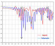
I am working on a rectifier using Schottky diode HSMS 2852 and a matching circuit. There is a difference between the layout and schematic results for S11 (between m9 vs m10 and m11 vs m12). How can I solve this problem to get better results?

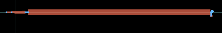
I have used TML for the input port as mentioned @volker@muehlhaus in his posts. I also used TML for the output port.

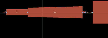
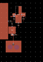
I have attached the layout and substrate screenshots. Please have a look.

Thanks very much.
 

Attachments

  • S11_layout.PNG
    S11_layout.PNG
    51.8 KB · Views: 47
  • layout_1.PNG
    layout_1.PNG
    3.8 KB · Views: 48
  • layout_2.PNG
    layout_2.PNG
    8.7 KB · Views: 46
  • total_layout.PNG
    total_layout.PNG
    1.3 KB · Views: 41
Last edited:

LaTeX Commands Quick-Menu:

Similar threads

Part and Inventory Search

Welcome to EDABoard.com

Sponsor

Back
Top