Continue to Site

Welcome to EDAboard.com

Welcome to our site! EDAboard.com is an international Electronics Discussion Forum focused on EDA software, circuits, schematics, books, theory, papers, asic, pld, 8051, DSP, Network, RF, Analog Design, PCB, Service Manuals... and a whole lot more! To participate you need to register. Registration is free. Click here to register now.

Why are poorly supported pcb layout packages so popular?

Status
Not open for further replies.
generally we need to save at different levels. and also save with some alternate name as backup so that we can avert such crashes.
these crashes are known. While working office and D-base etc, have always a guard copy, and a copy in another location like pen drive, CD etc are a must. Otherwise, a HDD crash cripples your files, unless you have skill or money to recover the contents.
 
  • Like
Reactions: treez

    T

    Points: 2
    Helpful Answer Positive Rating
Eagle is the scourge of the PCB layout consultancy fraternity....they hate it....because Eagle is so easy to use that customers of pcb layout consultancys could just do the jobs themselves by using eagle.... this is due to the tons of free www, youtube etc support that exists for eagle.

By the way, search the web , and you will find tons of unqualified slatings and slaggings of eagle...eagle is hated.....as it can reduce the wealth of those in the pcb layout business.
Which other PCB layout packages have this eagle like quality?.....ie theyre so easy to use, and so well supported , that they are a serious threat to the XXXXXX user fraternity, where "xxxxxx" is a high end pcb layout package.

"kicad" name comes up a lot here.

-Does it have ODB output?
-bus routing?
-automatic track collision avoidance (ie during track routing, tracks auto stop when they get nearer than the set clearance distance from different net copper.
-how much does it cost?
-does it have a free version?
-how limited (if at all) is the free version
-is kicad (pay version) limited in nodes, nets,layers ,board size?
-does kicad have a free viewer?
-dxf import and export
-3D capability
-3D mechanical enclosure collision avoidance.

**broken link removed**
..the kicad web page does not make seem to offer answers to the above
 
Last edited by a moderator:

Eagle is the scourge of the PCB layout consultancy fraternity....they hate it....because Eagle is so easy to use that customers of pcb layout consultancys could just do the jobs themselves by using eagle....

A bold statement. I don't think that any PCB service provider need to fear Eagle or other "easy" PCB packages. The main problem still isn't ruling the tool, it's mastering quality layout.
 

-Does it have ODB output?
Not natively at the moment but you can add your own scripts to do most things using Python language.

-bus routing?
Yes.

-automatic track collision avoidance (ie during track routing, tracks auto stop when they get nearer than the set clearance distance from different net copper.
Yes. It will stop you manually routing where it violates the rules you have set (or the defaults if you haven't set any) and the auto-router does it anyway.

-how much does it cost?
-does it have a free version?
-how limited (if at all) is the free version
-is kicad (pay version) limited in nodes, nets,layers ,board size?
The whole package is completly free and uncrippled. It supports up to 16 layers and as far as I know there is no node or reasonable board size limit. Schematics can be heirachical and spread across many sheets.

-does kicad have a free viewer?
It has a built in gerber viewer. With all the usual layer controls.

-dxf import and export
Not import (unless you script it yourself) but it can plot in Postscript, PDF, SVG, DXF and HPGL.

-3D capability
Full built in 3D board viewer with zoom rotate etc. Most devices have 3D models but you can build your own custom shapes using a link to 'Wings' program or any other of your choice.

-3D mechanical enclosure collision avoidance.
It will not allow component footprint overlaps without warning you but it has no height checking.

I've used it for several products, some quite complicated and PCB houses had no problems with it's output files.
Download it and look at the example files, especially the video board for a demo of what it can do.

Brian.
 

Thanks Betwixt.
It has a built in gerber viewer. With all the usual layer controls.
I was liking Kicad until I hear that it only has a "gerber viewer".....I like to have a free total viewer where I can see the net names etc, as the layout engineer made them........Eagle has this ability.......ie with Eagle, you basically have the use of the full eagle layout and schematic package in viewer mode, and this is totally free.....the viewer is free even if the board has 16 layers etc etc.

DXF import is possible with eagle using software provided by third parties...that sounds easier than in kicad, where it appears from your kind reply, that one needs to learn a scripting language.

I am wondering how long kicad has been around?.....I didn't hear too much about it when I was choosing a layout program for my last job.
 

Interesting comparisons, but as posted earlier, for a small company or professional individual Eagle is NOT free and the useful version starts at quite a high cost for the limitations imposed.

Although it has not been around for so long and in some areas not currently as powerful, DesignSpark PCB is for me the best "free for commercial" use PCB design package that I could find. It has a huge board area (I needed to exceed the lower cost Eagle packages board limits) and many layers (although I only need 4 at present).
It has a rapidly growing number of users and being adopted by educational establishments around the world and smaller companies.
I have also found their email support excellent and fast, plus they seem to be churning out tutorial items at a rate of knots.

As said once you get into the "commercial arena", the free package choices change from hobbiest options.
 
  • Like
Reactions: treez

    T

    Points: 2
    Helpful Answer Positive Rating
Sorry if I mislead you. The Gerber viewer is there to see the finished artwork as it would be presented to a PCB fabricator.

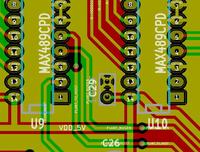
The schematic is fully 'labelable' (if that's a word) with net names and they are transferred to the rats nest and traces in the PCB layout part of the program. I've attached a screen capture of a section of a board I've just made so you can see. Most of the nets were just given default "N-xxxxxx" numbers by the program but some were named on the schematic and you can see they are carried to the PCB. If you zoom right in, it will put the net name on the pad itself. It also has all the usual net highlighting and flood fill functions and exports netlists to various simulators and even to "Freerouter" the on-line router although the one built in is as good as any I've seen.

I'm not sure exactly when it was first released, it was around 10 years ago.


Brian.
 
  • Like
Reactions: treez

    T

    Points: 2
    Helpful Answer Positive Rating
I would advise against settling for designspark.
 
  • Like
Reactions: treez

    T

    Points: 2
    Helpful Answer Positive Rating
I would advise against settling for designspark.

Why? A rather bland statement! I have been successfully using it since V3 (now on V5) with excellent results with professionally manufactured PCBs for my small production runs.

Its features compare well with other packages I have used (paid for and free) and it's not tied into any PCB manufacturer so no "got you" catch.

Using the wizards I have quickly and easily built up my own library of parts so these meet my needs.
I do manual routing as I've never found a router which does analogue layout as I require and in DSPCB this works well in manual routing for me.

So for its balance of features, free for comercial use, no small board size limits, no PCB house tie in, good email support and web tutorials, I can only advise 'give it a try'.

It may not be perfect but what is? Look at the forums for all the different products and from the most active to the least there is the "how do you....", "why can't I...", "It doesn't do it the way I want", "Why doesn't it do....", but put in a bit of effort and learn the features and most packages are quite capable and DSPCB certainly is for me.
 
  • Like
Reactions: treez

    T

    Points: 2
    Helpful Answer Positive Rating
I've tried various packages too and am really starting to like Designspark for the ease of use. Since I tend to need to use a lot of odd-ball parts (mostly connectors), the first thing I check is how easy it is to make a new component. So far, Designspark is the easiest. Draw a schematic symbol (or re-use ANY schematic symbol), draw the PCB footprint (pick some pads, type in the coordinates or manually place), create the component by matching the schematic pin to the footprint pin.

I'm not looking to create multi-layer microprocessor boards. I have access to Altium if I need to do that. I'm looking for something to do relatively simple designs and get them to MY board house quickly.
 
  • Like
Reactions: treez and pinout

    pinout

    Points: 2
    Helpful Answer Positive Rating
    T

    Points: 2
    Helpful Answer Positive Rating
Kicad does sound very good, I cant understand how they can afford to do it completely for no charge? its totally free?
 

It was started as a teaching aid for programmers at a French University but being open source, it quickly gathered support from other users. Almost everything is done voluntarily but it does have some financial aid from CERN. It's a very stable and widely respected product and unlike most systems, it is cross-platform so for example I can develop something on a Linux or Mac machine and transfer it to a Windows machine or vice versa.

The nice thing about open source is it gets improved by real users and almost in real time. Although new 'stable' versions are released every few months, you can download and test new development versions every day. If something doesn't work quite right or you can see a way to improve it, you can fix it yourself or tell the development team and they fix it as quickly as possible for you. Also, not being tied to a single development company (or component retailer!), it stays available and updated even if they go bust or get swallowed up by a competitor.

It's interesting that there are many converters on the Internet to read other CAD system files and convert them to Kicad - but almost none to do it the other way around, go figure :shock:

Brian.
 
  • Like
Reactions: treez and FvM

    FvM

    Points: 2
    Helpful Answer Positive Rating
    T

    Points: 2
    Helpful Answer Positive Rating
Well KiCAD does sound very good.....from your last statement I bet I know what the high end PCB package vendors are thinking......."lets buy out KiCAD's software engineers and tell them to stop developing kicad because its a threat to our profits".

As soon as they start loosing customers and money to kicad,.... that will happen, and none of our politicians will take any interest.
 

Again, that's another advantage of open source programs, you can download the entire source code and compile it yourself, the instructions are included! There are no Kicad software engineers as such, it's all done by volunteers who presumably have 'day' jobs as well. If one steps down, someone else takes their place and they are distributed around the World. Think of it as a colaborative effort by maybe 20 core software writers and hundreds of contributors but working under a single team leader. Having access to the source code also means it's impossible to hide any tracking, virus or trojan routines in it too!

Brian.
 
  • Like
Reactions: treez

    T

    Points: 2
    Helpful Answer Positive Rating
The most widely used PCB design packages though are those produced by:
Mentor, Zuken and Cadence...
And all have a pay for maintenance service, so that you can get almost instant access to a help desk and technical support.
 
  • Like
Reactions: treez

    T

    Points: 2
    Helpful Answer Positive Rating
And all have a pay for maintenance service, so that you can get almost instant access to a help desk and technical support.
..maybe the bigger customers get that good treatment, but i was with one of them as a "singley", and didnt get much support, even though i'd payed the licence & maintenance and everything.
 

Don't know which package you had, but I have had no problems in the past as a customer with all the main packages, at different sized enterprises from small to large...
 
  • Like
Reactions: treez

    T

    Points: 2
    Helpful Answer Positive Rating
I've tried various packages too and am really starting to like Designspark for the ease of use. Since I tend to need to use a lot of odd-ball parts (mostly connectors), the first thing I check is how easy it is to make a new component. So far, Designspark is the easiest. Draw a schematic symbol (or re-use ANY schematic symbol), draw the PCB footprint (pick some pads, type in the coordinates or manually place), create the component by matching the schematic pin to the footprint pin.

I'm not looking to create multi-layer microprocessor boards. I have access to Altium if I need to do that. I'm looking for something to do relatively simple designs and get them to MY board house quickly.

Totally agree! I have now mastered the library manager and the package works very smoothly, this is simple once you make the effort to learn.
The support forum has been helpful, but since the launch of DS Mechanical 3D has been a bit busy, but responsive.
For me, with no commercial restrictions it just right.

I think beginners should be pointed at the library tools and understand that before diving in as they would get up to speed quicker.

Finished and populated my double sided manually routed SM board, now looking at 4 layers....
 

So you can get 3D including 3D collision avoidance with designspark?
Is designspark free?

Out of Kicad, designspark, diptrace, eagle, -which if these have dxf import, as well as 3D PCB viewing, and 3D PCB collision avoidance inside the enclosure?

Without dxf import, at least, i'd say any pcb layout package will, rightly or wrongly, never get accepted by industry.

On a serious note, just listen to us all, each of us declaring the superiority of one package over another, .....this is what is happening in industry today, and is why very few hardware engineers have got a clue about how to use a pcb layout package.

I still say that mostly due to the hobby fraternity uploading tutorials etc on the web , and offering general froum support.......eagle is the easiest to use.

I mean, its those fiddly problems like you're trying to measure from one pad to another, and the package keeps snapping to the wrong outline, even though thats not the nearest outline......trying to solve these kind of problems with the manual can be horrendous.

I used one package, and i used to go to forums and ask, and all i got was "its all in the manual".

I have no connection to eagle, if it disappeared and some other package came in with the same degree of "idiot's support", then i'd be happy with that.

It seems to me that PCB layout packages have flourished in a chaotic way, and industry is suffering from the mess.....most managers are clueless which one to choose, and so just choose one with as many features as possible, in the hope that it wont be deficient in any respect.
 
Last edited by a moderator:

Status
Not open for further replies.

Part and Inventory Search

Welcome to EDABoard.com

Sponsor

Back
Top