Bobson2000
Junior Member level 3

- Joined
- Aug 23, 2023
- Messages
- 25
- Helped
- 0
- Reputation
- 0
- Reaction score
- 0
- Trophy points
- 1
- Activity points
- 346
Hi. Im design PCB with FPGA. I want to place data traces between FPGA, and SFP module. Signals are of course differential, i have one RX, and TX signal for each SFP.
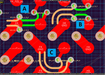
I lead the paths from the FPGA through microvias to layer 3 or 5 (2, 4 and 6 are GND). I know that I should also add antipads and ground vias next to the signal vias. However, I wonder which solution will be better and will result in fewer impedance discontinuities and signal losses. I have 3 options (A, B, C) presented in the graphic and I wanted to ask which one is better? One of the options includes grommets on the pads, which is not the best idea, but it should not cause a problem - perhaps they can be placed centrally on the pads - maybe even necessary? In variant C, the vias are one on top of the other, so due to the fact that they are a micro via (1->3 and 3->5), there is a ring on layer 3 - in variants A and B there is no such problem, but there are two " "via passes" and the number of such passes should be minimal. Please give me your opinion. Currently, my goal is an SFP operating at 1Gbit/s, but if I can make changes to the layout that allow me to try to run 10Gbit/s, I will gladly implement them. I don't plan to change the laminate - currently FR4 with one of the denser prepregs. I readed couple of documents about it, but i have no experience in real life with this speeds.
Thanks

