Continue to Site

Welcome to EDAboard.com

Welcome to our site! EDAboard.com is an international Electronics Discussion Forum focused on EDA software, circuits, schematics, books, theory, papers, asic, pld, 8051, DSP, Network, RF, Analog Design, PCB, Service Manuals... and a whole lot more! To participate you need to register. Registration is free. Click here to register now.

Voltage Spike problem

Status
Not open for further replies.
I think also need to look at Vgs and Vds from the the OTHER FETs as well. It looks like maybe you've got some timing issue between the two channels. (One channel turning on before the other one has turned off).

Also, it's not clear WHAT that bottom plot is showing; please explain. But if that's showing spikes on your power supply then you're either picking up junk on your scope ground lead, or you haven't properly decoupled the power supply.

What's your load?

And those 100pF caps seem awfully small for their intended purpose; you've got a lot of power to deal with here and 100pF can't store a whole lot of energy.
 

You must have caps right by your fets - soldering these in as a lash-up you will see n your scope how this improves turn off ...

what caps do you mean?
Do you mean input caps for example c3 and c4 in this circuit?
2.PNG
and how close should they be?

- - - Updated - - -

I think also need to look at Vgs and Vds from the the OTHER FETs as well. It looks like maybe you've got some timing issue between the two channels. (One channel turning on before the other one has turned off).

.

If it is a timing issue, why Vgs and Vds are ok at no load?

Also, it's not clear WHAT that bottom plot is showing; please explain. But if that's showing spikes on your power supply then you're either picking up junk on your scope ground lead, or you haven't properly decoupled the power supply.

It is the SG3525 and HCPL3120 supply voltage. the supply voltage has no spike at no load.


What's your load?

It is bulb lamp.

And those 100pF caps seem awfully small for their intended purpose; you've got a lot of power to deal with here and 100pF can't store a whole lot of energy.
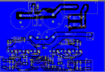
Sorry, i forgot to change the values in schematic. i've used two 220nf ceramic caps.
 
Last edited:

If it is a timing issue, why Vgs and Vds are ok at no load?
.
Because there's no current flowing when there's no load.

It is the SG3525 and HCPL3120 supply voltage. the supply voltage has no spike at no load.

This would indicate a decoupling problem or a power-supply that can't handle the load.
 

This would indicate a decoupling problem or a power-supply that can't handle the load.

I think also need to look at Vgs and Vds from the the OTHER FETs as well. It looks like maybe you've got some timing issue between the two channels. (One channel turning on before the other one has turned off).

There are electrolytic and ceramic caps right by each three ICs, so I don't think it is a decoupling problem.
these are Vgs and Vds and ICs supply voltage.

1.jpg2.jpg

How can i be sure that ICs supply voltage effects on MOSFETs or vice versa?
 

Label your plots; we have no idea what trace is what.

But it sure looks like the negative transitions are causing problems with your power rail, assuming that's what that top trace is.
 

barry said:
Label your plots; we have no idea what trace is what.

The blue trace is ICs supply voltage in both images.
the left image, purple and yellow traces are Vgs.
the right image, purple and yellow traces are Vds.


see post #6 ...

I have soldered 2uf film cap on the bottom layer right by the FETs, but it didn't work.

Capture.jpg

these are FETs. (marked as yellow)
 
Last edited:

You have a HUGE 170V spike at turn off. This definitely indicates a large inductance somewhere in your circuit. It's apparently a large enough spike to turn on the other FET. Those film caps might be the source of the inductance.
 

What are those diodes? if there is no change you must be picking up noise on your scope - put croc clip and probe to the same point ( i.e. shorted ) and connect to various points - if you see noise your scope is picking up CM RFI ...

- - - Updated - - -

the spike is at turn off - so wiring inductance and lack of quality caps close by to soak current up is the root cause ....

please advise operating conditions - type of fets and any parallel diodes ...

- - - Updated - - -

Just to clarify - the caps go across the supply rails - right by the fets.

it may now be time to try snubbing too - 1nF & 47E across each fet - very short leads ...
 
Hi,
I finally somewhat resolved the spike issue.
by changing the Gate-Source resistor, gate resistor and snubber values.
But now I have efficiency probelm.
the efficiency is about 60 percent.
for example, when the output power is 128 watt, the input power is 204 watt.
I measured the Vds and voltage of the output diode bridge.
each diode has about 10 volts on conducting.
when the output power is 520 watt, the input power is 828 watt.
in this case, each FET also has about 10 volts in on state.
the FET models I have used are irfp4568 and irfp260n.
what is the problem?
 

Since you supplied zero information, Ill just guess that you’ve slowed down the turn on/off and are losing power across the fets
 

The problem is in the simulation - without full detail - no helpful answers can be given.
 

The problem is in the simulation - without full detail - no helpful answers can be given.
This is Vds when the input power is about 400 Watt.
5.jpg

This is Vds when the input power is about 600 Watt.
2.jpg

This is Vds when the input power is about 800 Watt.
There are about 5 Volts across the Fet on conducting duration. and it increases by time.
4.jpg

The Fets are irfp260n in this test. is it ok for this topology?


The diodes are uf5408 in this test and this is the diode voltage.
8.jpg

there are about 15 volts across the diode on conducting duration.
7.jpg

I have used 2sb882 as NPN type and 2sd772 as PNP type for driving the fets instead of hcpl3120.
the Gate resistor is 24 ohms in this test. the lower gate resistor causes higher voltage and current spikes. also, I changed Rg to 7.5 ohms but the efficiency doesn't make any difference.

The inductor model is t184-26. this is the inductor voltage.
6.jpg
 

..........

- - - Updated - - -

See post # 16 you must have 1uF or bigger frm +HVDC to 0v right by the fets....

you can see that it is turn off that is the problem - no where for the turn off current to commute to if there are no good film / foil caps near the fets ...

- - - Updated - - -

sorry - where is the schematic ... ?
 

looking at the waveforms - push pull - you have a fair bit of leakage L in the Tx - you can see this at the turn off - it looks like your supply is soft - how much uF on Vin? do you have film/foil caps right on Vin right by the fets?

- - - Updated - - -

what value is your o/p choke?
 

looking at the waveforms - push pull - you have a fair bit of leakage L in the Tx - you can see this at the turn off - it looks like your supply is soft - how much uF on Vin? do you have film/foil caps right on Vin right by the fets?

I soldered two 1uf film cap as close as possible to fets across Vin.
There are two 4700uf bulk caps and two 220 nf cermic caps on Vin.
what value is your o/p choke?
its 600uH t184-26 core.
I have efficiency problem. Has it something to do with spike?
 

Well then - it is clear you have way too much leakage L int he Tx - can you measure or post a sketch of the construction ?
 

For push - pull with a bad transformer you will need aggressive snubbing across the fets/igbt's ... can you post a schematic?
 

Status
Not open for further replies.

Similar threads

Part and Inventory Search

Welcome to EDABoard.com

Sponsor

Back
Top