rayansyd
Newbie level 5

- Joined
- Oct 1, 2024
- Messages
- 8
- Helped
- 0
- Reputation
- 0
- Reaction score
- 0
- Trophy points
- 1
- Activity points
- 64
Hi everyone,
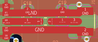
I'm a beginner in PCB design, and I've been working on a coplanar waveguide (CPW) structure for an RF signal on my PCB. Here are the details of my design:
I'm currently at the stage of adding via fencing to this CPW structure and need some advice. Specifically, how much clearance should I maintain between the vias and the edge of the RF signal trace to ensure effective shielding and optimal performance?
Any guidance or tips would be greatly appreciated
I'm a beginner in PCB design, and I've been working on a coplanar waveguide (CPW) structure for an RF signal on my PCB. Here are the details of my design:
- Signal Trace Width: 1 mm
- Clearance for 50 Ohm Impedance Matching: 0.2 mm
- Board Length: 50 mm
I'm currently at the stage of adding via fencing to this CPW structure and need some advice. Specifically, how much clearance should I maintain between the vias and the edge of the RF signal trace to ensure effective shielding and optimal performance?
Any guidance or tips would be greatly appreciated
