Continue to Site

Welcome to EDAboard.com

Welcome to our site! EDAboard.com is an international Electronics Discussion Forum focused on EDA software, circuits, schematics, books, theory, papers, asic, pld, 8051, DSP, Network, RF, Analog Design, PCB, Service Manuals... and a whole lot more! To participate you need to register. Registration is free. Click here to register now.

Verification of openEMS modeling with real-world using LibreVNA

oberstet

Newbie level 6
Joined
Feb 1, 2024
Messages
13
Helped
0
Reputation
0
Reaction score
0
Trophy points
1
Activity points
210
Hi all,

as a RF newbie, I've been making some progress starting from EM modeling, having first PCBs designed and manufactured, but I am now stuck just before "closing the loop" with real-world measurements using LibreVNA =(

any help or hints would be greatly appreciated!

Cheers,
/Tobias

------

sorry if this all seems pretty basic, or even stupid or wrong: I am actually a SW engineer, and with RF and PCBs, I am really in a world very different from what I'm used to and new;)

anyways, my _plan_ for verifying my "modeling-to-realworld" workflow was the following:

1. model the PCB stack (2-Layer Teflon/PTFE) of the manufacturer (JLCPCB) I selected in openEMS - DONE!
2. use an impedance calculator for computing the PCB trace width for a single-ended 50R trace - DONE!
3. purchase LibreVNA and test fixture enclosures - DONE!
4. design a most simple PCB tile with a single 50R microstrip trace and with width 1.3mm - 2.4mm - DONE!
5. have those PCB tiles manufactured and mounted into the test fixtures - DONE!
6. calibrate LibreVNA using the included calkit and then measure S11 for PCB trace width 1.3mm and 1.9mm, and the calkit THRU - DONE!

pls see further below for screenshots.

my problem is: it "looks" good (that is, 1.9mm is actually "best" also in real world measurements), but I'm not sure!

also, at least rgd "phase", the results between CalKit-THRU and 1.9mm PCB trace look different. Is that because my PCB trace has 50+mm length (rather than "almost 0")?

the actual question I want to answer is:

Of all PCB trace widths I have (1.3-2.4mm), is 1.9mm indeed "the best" (rgd match to 50R)?

If so, that would mean: my modeling/simulation matches the real world (with PCB from my manufacturer and measuring using my VNA).

This would give me some reason for confidence that what I model and simulate in openEMS actually corresponds to the real world.

How do people usually do that? I mean: establish confidence in EM-model-to-real-world matching?

-----

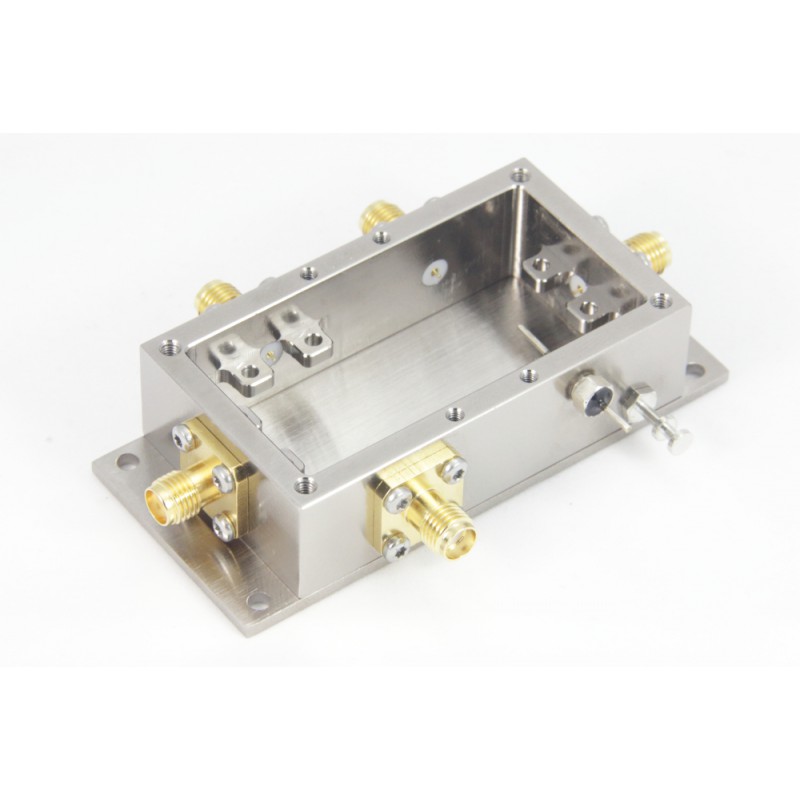
PCB trace tiles and test fixture:

PXL_20240315_102834194.jpg


PXL_20240408_114849992.jpg


-------------

LibreVNA / etc measurement setup:

PXL_20240426_112328696.jpg


-------------

Results for LibreVNA Calkit THRU:

CAL-THRU-Screenshot from 2024-04-26 13-18-26.png


-------------

Results for my PCB trace in test fixture with width 1.9mm:

TRACE-1.9mm-Screenshot from 2024-04-26 13-15-06.png


-------------

Results for my PCB trace in test fixture with width 1.3mm:

TRACE-1.3mm-Screenshot from 2024-04-26 13-13-34.png
 
Nice job on the PCBs, they look great.

"The best" is of course subjective. What are your actual criteria? The return losses look decent over the measured frequency range, but only you know what you need...

Yes, the length of the line causes extra phase to be incurred.

How do we establish confidence? Compare simulated data to measured data. The simulation is ideally a duplicate of everything you have in reality, up to the SMA ports. Extract the same scattering parameters from the simulation and you should be able to assess your confidence.

Have you simulated the PCB in the enclosure? At the frequency range you're measuring, the conductive enclosure could cause some gnarly effects. Especially with a lid.
 
Hi Tobias,

in your measurement you need to make sure that there is no gap in ground at the location that I marked with the arrows. Ideally you would solder the backside ground to the connector body or box, but it seems that your box can't be soldered. Some copper foil should be good enough then.

If ground current can only flow through the screws that are left and right from the line, that is a massive detour for ground path current, resulting in series L at the connector-PCB interface.

no_gap_please.jpg
 
Nice job on the PCBs, they look great.

"The best" is of course subjective. What are your actual criteria? The return losses look decent over the measured frequency range, but only you know what you need...

Yes, the length of the line causes extra phase to be incurred.

How do we establish confidence? Compare simulated data to measured data. The simulation is ideally a duplicate of everything you have in reality, up to the SMA ports. Extract the same scattering parameters from the simulation and you should be able to assess your confidence.

Have you simulated the PCB in the enclosure? At the frequency range you're measuring, the conductive enclosure could cause some gnarly effects. Especially with a lid.

Thank you so much for your feedback and thoughts!

rgd PCB: yeah, I am "medium-happy". this is my very first PCB, and for 1 iteration, I guess I should be "happy".

basically, the only problem I encountered is wrt to the material: I mean, the mouse bites are good and do work, but I didn't know that the Teflon/PTFE PCB material is basically like chewing gum! so while the mouse bites do break at the right path, you still need a cutter. anyways, works for me.

> What are your actual criteria?

My criteria is:

*Effective impedance (as measured) for 1.9mm trace width is 50R +/- "tolerance" (ideally, within manufacturer tolerance for thickness and trace width)*

If I can establish this in real world, that would fit my EM modeling and calculations perfectly.

> Yes, the length of the line causes extra phase to be incurred.

Right, thanks! Got it.

> The return losses look decent over the measured frequency range

Thanks for confirming! I wasn't sure .. first time newbie;)

> the measured frequency range, but only you know what you need...

I need the frequency range 400 MHz to 2.8 GHz, and I decided to use a range of 300 MHz to 3 GHz for VNA calibration and measurements. The VNA should work up to 6 GHz.

I do have a LPDA antenna model in openEMS which looks good for above range, and I now want to have that antenna in real;)

Ideally, since I now know my way around within the simulator, I'd like to verify and calibrate to real-world PCBs _once_, and then basically work within EM simulations "only", and then only order PCBs once and have it match perfectly in real-world measurements.

I am doing all of this the first time, so I expect "some learning" curve. No problem. But I want to systematically *verify this workflow* and be good;)

> Have you simulated the PCB in the enclosure?

No, I haven't, only the PCB trace without enclosure and SMA. But the manufacturer of the enclosure did, I am using:


I have closely modeled the PCB along designs by that manufacturer - which was optimized for the combination of enclosure and SMA jack used.
--- Updated ---

Hi Tobias,

in your measurement you need to make sure that there is no gap in ground at the location that I marked with the arrows. Ideally you would solder the backside ground to the connector body or box, but it seems that your box can't be soldered. Some copper foil should be good enough then.

If ground current can only flow through the screws that are left and right from the line, that is a massive detour for ground path current, resulting in series L at the connector-PCB interface.

View attachment 190389

Hi Volker,

thank you so much for feedback and hints!!

this is a crucial phase for me .. first time taking the workflow from EM model to real world;) and I have zero experience, hah.

> your box can't be soldered

nope, it is ALU .. this:


> If ground current can only flow through the screws that are left and right from the line, that is a massive detour for ground path current, resulting in series L at the connector-PCB interface.

I closely followed the PCB design at the ports end that the manufacturer is using (for some demo board). Let me post a couple of pics including the SMA jack etc

I'm not sure how I could do what you seem to hint at .. the SMA jack GND has full circular connection to the complete enclosure (which is GND), and only the SMA jack pin extends into the enclosure and is soldered to the trace end (which has a fixed width, and only starting from the small solder mask rectangle to the right/left, I am using different trace width then (of length 51mm) )

Here are more pics with some details (I removed the metal bridge/head crossing the port .. this is all GND)

PXL_20240426_155736182.jpg


PXL_20240426_155825214.MP.jpg

--- Updated ---

Hi Tobias,

in your measurement you need to make sure that there is no gap in ground at the location that I marked with the arrows. Ideally you would solder the backside ground to the connector body or box, but it seems that your box can't be soldered. Some copper foil should be good enough then.

If ground current can only flow through the screws that are left and right from the line, that is a massive detour for ground path current, resulting in series L at the connector-PCB interface.

View attachment 190389

One more Q: if you look at the result from my soldering

1714156450309.png


this is certainly not perfect.

I mean, too much solder I guess?

Does it matter? (for 400M to 2.8GHz .. nothing extraordinary)

I recognized that while soldering, but I lack proper "add ons" .. like what is that called, "Flux"? and then also some "desolder / solder removal" tape or what.

How is that stuff even called? I can order missing stuff .. but I'd need to know what I need and what to order;)
 
Last edited:
> If they touch the side wall that would be perfect.

I double checked (see pics below), and it indeed might be a mistake: me mounting the metal brackets _not_ in the right 180° orientation .. there is a very small gap .. I need to check whether I am able to screw the brackets turned around .. that might lead to "0 side wall to bracket" distance.

thing is, screwing this stuff is "tricky" for someone only used to hit RETURN all day long;)

I will check that. I want to do it right.

thanks!!

PXL_20240426_185959206.jpg


PXL_20240426_190323149.MP.jpg


PXL_20240426_190248910.jpg
 
No, I haven't, only the PCB trace without enclosure and SMA. But the manufacturer of the enclosure did, I am using:
The central trace can interact with the enclosure, even with a solid connection between your other PCB traces and the enclosure. In the worst case, this could cause your system to operate more like an antenna or filter. It's unlikely, but best to check in simulation if possible. Simulation with the enclosure is part of any good RF deign process.
One more Q: if you look at the result from my soldering
Yes, I would say there is too much solder; the solder should be flat (or as otherwise specified by the connector manufacturer, there are often instructions in the datasheet). Use braided solder wick to remove some of it for best results. At ~3 GHz, you could see a difference in the response.
 
I reviewed the thread and didn't see a target S11 or VSWR specification for the design. Even perfectly mounted RF connectors involve a certain amount of reflections. So hard to say if your design is bad, good or even over-engineered. May be your spec is "as good as possible"?
 
I reviewed the thread and didn't see a target S11 or VSWR specification for the design. Even perfectly mounted RF connectors involve a certain amount of reflections. So hard to say if your design is bad, good or even over-engineered. May be your spec is "as good as possible"?

I am coming from this world, yes indeed;) actually, I am coming from: "as good as conceivable". That is "all frequencies at 0 S11". But I learned from others and from my simulations that this is unrealistic.

I want to have a real-world antenna (actually, a phased array of 4 elements) for "optimum" defined as:

400 MHz to 2.8 GHz with at S11 at least -10dB over the whole range without gaps

I do have an antenna model simulated in openEMS which _almost_ achieves that. I'll post some pics below.

The remaining main problem is the bump around 1.5 GHz. This is due to the main feed line design of my LPDA. And it depends on the exact PCB stackup.

Because of that, before fixing the remaining main problem (as well as the slightly suboptimal regions), I decided to _first_ close the simulation-to-realworld loop at least once;) I never did any PCBs or RF before.

And to do that, I first wanted to close the loop not for the whole LPDA thing, but for the _most simple_ scenario I could use to verify - which is 50R single-ended traces.

Once I have that and feel confident, I need to do "Double-sided Parallel Stripline" (DSPSL) - which my LPDA main feedline actually is .. I guess - and "Balanced-Unbalanced" elements - ideally doing sth like this: https://www.hindawi.com/journals/ijap/2013/921859/

Once I have that, I can do the LPDA verification - that is all S11 centric.

Once I have that, I will do radiation pattern, and most importantly, LPDA element phase matching.

Then I'm done and can move back to my home field, bits and code and RETURN and all that;)

That's the plan;) Currently. It is quite a ride though, so thanks for any help, hints or plain feedback!! as mentioned, I am in a totally new and foreign world ..

1714406434392.png


1714406465319.png

--- Updated ---

just noting, the titles in the S11 charts are wrong, it is and LPDA, not a dipole ... something like the following (I do generate the geometry from code and parameters .. so I forgot if that exact design matches above exact graphs .. but it doesn't matter)

1714406938172.png
 
Last edited:

LaTeX Commands Quick-Menu:

Part and Inventory Search

Welcome to EDABoard.com

Sponsor

Back
Top