Continue to Site

Welcome to EDAboard.com

Welcome to our site! EDAboard.com is an international Electronics Discussion Forum focused on EDA software, circuits, schematics, books, theory, papers, asic, pld, 8051, DSP, Network, RF, Analog Design, PCB, Service Manuals... and a whole lot more! To participate you need to register. Registration is free. Click here to register now.

trace noise in opamp circuit

yefj

Advanced Member level 5
Joined
Sep 12, 2019
Messages
1,505
Helped
1
Reputation
2
Reaction score
5
Trophy points
38
Activity points
9,114
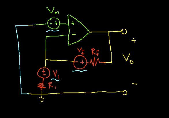
Hello, In this video we represent each component as a source of noise,but in real life the traces also play a role.
How can we simulate noise with the contribution of the traces connecting the components?
Thanks.
1707073629883.png
 
Hi,

in a schematic "traces" are considered ideal.

For sure in real life that are not ideal.
But they don´t really generate much moise by themselves. They rather suffer form magnetically or capacitively induced noise. This means "noise from somewhere else".
So you need to find the real noise source. ... and the way how it becomes induced. This absolutely depends on PCB layout.
Thus you need to verify the PCB layout.

Klaus
 
Hello Klaus , so if I understand you correctly you say to do VIA shielding surrounding the traces ?
Is there some more tips regarding refusing noise from traces ?
Thanks .
 
so if I understand you correctly you say to do VIA shielding surrounding the traces ?
...why not remove the true nose source?

also the power supply plays a role...

What I wanted to say: There is more than just the schematic that influences the noise. It´s also all that surrounds the circuit and how the PCB looks like.

Klaus
 
There are many sources of noise, Input referred internal, Resistive Thermal and external noises radiated as well as parasitic conducted noise such as voltage from ESL. V=LdI/dt or Ic=CdV/dt from parasitic capacitance if adequate conditions exist.

 
Hello , I want to focus on the traces part of minimising noise on the output.. You 1.recommend me to shield the traces to eliminate noise coupling to them ? Correct?
2. Another important thing I can’t understand is it’s recommended to make traces short as possible ,place passive compononents as close as possible to the OPAMP input .
Because other wise fast opamp will have parasitic capacitance .
From signal integrity I know that long traces create inductance , how come long traces create capacitance on the input on the opamp?
Thanks .
 
Most new good datasheets., for wideband fast parts, have layout recommendations in them
as well as bypass recommendations.


Regards, Dana.
 

LaTeX Commands Quick-Menu:

Similar threads

Part and Inventory Search

Welcome to EDABoard.com

Sponsor

Back
Top