Continue to Site

Welcome to EDAboard.com

Welcome to our site! EDAboard.com is an international Electronics Discussion Forum focused on EDA software, circuits, schematics, books, theory, papers, asic, pld, 8051, DSP, Network, RF, Analog Design, PCB, Service Manuals... and a whole lot more! To participate you need to register. Registration is free. Click here to register now.

TL494 Half Bridge blowing fuse

Status
Not open for further replies.
Hi thanks for the reply. Effectively i feel its the scope bandwidth the new one which is on its way should solve this problem. I can effectively post a new schematic of the current SMPS here for easier diagnostics. Just a simple question which CAD software has a built in model of TL494 in it? Or is there a way to get a TL494 spice model somewhere on the net??? Thanks
 

can you post your latest schematic, and you mentioned transformer calculations, please include them also
 

Hi, really sorry for this very late reply i was taken up completely with my job at the office. I have attached the latest schematic TL494 SMPS.jpg. The BC556 is actually 2SA733 i could not find it in eagle. I will get my gate transfo calculations and post it here
 

I see two problems, that may explain erratical behaviour of the converter.

- As already mentioned by other contributors, the gate and output voltages are more trapezoidal than square waves. I assume, these are the real waveforms and not results of a slow oscilloscope or intentional filter settings. I think, the slow edges are designed into the circuit. You have e.g. C9 and C10 increasing the rise time of the opposite channel.

- The breadboard design is involving considerable wiring inductances. There's a high risk, that you'll get parasitic oscillations during turn-on or turn-off of the MOSFETs, that may easily destroy the transistors. A particular voltage and/or current level would be needed to trigger the oscillation.
 

Hi Fvm thanks for the reply could you please develop your point about
"A particular voltage and/or current level would be needed to trigger the oscillation. " I would be eager to learn more thanks. I have no choice than to use project board its still a non working design on its way to improvement. I preferred this instead of beadboard which was worse and loosee
 

Q1,2 should be BC337 or equiv (for speed), and Q3,4 should be BC327 - same reason, C9,10 should be 1nF max, R5,6 to 680ohm, there should be a 470nF cap in series with the pri winding of your gate drive transfomer, ideally Q5,6 should be BC327 or equiv to get a decent turn off. This may help get a good gate drive waveform, Regards, Orson Cart.
 

I used the term "breadboard" for your vero-like "project board". Whatever you call it, the photo shows rather long connection wires. You didn't show the bottom side, but I won't expect extensively spread ground connections.

If the problems start above a certain voltage level, I don't see a chance but increasing the supply voltage continuously. Hopefully, you see some effect before fatal damage ocurs.

P.S.:
Q1,2 should be BC337 or equiv (for speed), and Q3,4 should be BC327 - same reason
The BD types are effectively in the same speed class.
 

Hi Zeus
thanks for reply but I CAN NOT open the figure ?? something wrong! please rescan and re send !
 

The BD types are effectively in the same speed class

Only the philips/nxp type have a decent fT ~ 190Mhz, all other makers class them as general purpose and don't even show an fT on their data sheets, we have found the generics pityfully slow compared to the philips/nxp. Regards, Orson Cart.
 

Hi thanks for the reply. Nebo it could be due to your browser settings check your flash compatibility it could be due to it. Regarding the transistors i do have BC337-327 handy i can change them or 2Sc945 and 2Sa733 or BC546B and BC556B. You can tell whichever is best i will try it. I am not sure i can get ZTX transistors here but i could check. Orson regarding the values you have suggested i will apply them. Regarding my gate drive transfo until i get back the full calculations, this is how i remeber i did it-> Find the EEl16 AL Value, target for a 2mH inductance for 50KHZ frequency and calculate the turns from there using N=SQRT AL/.... something like that.

For the main EI-33 core i've used N=VCCx10e8/4FBMAX something like that i will confirm the formula and the values i've used and post them here today.
 

Only the philips/nxp type have a decent fT ~ 190Mhz, all other makers class them as general purpose and don't even show an fT on their data sheets, we have found the generics pityfully slow compared to the philips/nxp.
These things happen. Any reason to be sure about BC327/BC337?

---------- Post added at 11:41 ---------- Previous post was at 11:33 ----------

i do have BC337-327 handy i can change them or 2Sc945 and 2Sa733 or BC546B and BC556B
All these are 100 mA class, not actually suited for the purpose. I think, you should better keep BD139/140 for the time being. As long as drive the output drivers with TL494 emitter output and about 1k load resistors, you don't need to think about faster transistors, I fear.
 

Ok Fvm i will keep them. Regarding the main transformer calculation i have used 382V x 10 power 8 / (4X 50KHz X 2000 Gauss X 1.3 CM Square cross section area ) = 73 turns primary

For secondary turns i have used 1.1 * [35V (secondary op) + 2V (Fwd rectifier vdrop)]/ [262 Vdc (Vin low) - 2V (Fwd rectifier vdrop) X 50/100 (Max Duty Cycle TL494) ] = 23 turns secondary

For gate drive transfo I have aimed for 2mH inductance for 50KHz using the following : N=SQUAREROOT( inductance/ AL)= SQUAREROOT(2mH/ 800)=100 Turns primary. For 1:1 turns ratio 100 Turns secondary.

If ever there is any error in my calculations please let me know. Thanks
 

Any reason to be sure about BC327/BC337

We use them in our 2.4kW off line converters, for the gate drive transformers and for the gate turn off (40nS).

It would be advantageous to buffer the 494 o/p's with a CMOS gate to give square edges before applying to the gate drive buffers.

Regards, Orson Cart.
 

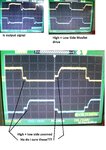
Hi i got my new DSO today and the issues are clearer now its related to the gate drive signal. Any help on how i can improve the signal. P.S: the waveforms are for the latest schematic i sent. No component has been changed yet. pic.jpg.

By the ay can anybody confirm if my calculations are correct? At least i can eliminate the magnetics from the problem.

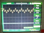
The waveform coming out of the current sense transformer looks like this pic2.jpg
 
Last edited:

Really weird. The driver circuits manages to operate the MOSFETs in lossy linear mode, possibly even both at the same time.

To understand the problem, you should also watch the waveforms at the transformer secondary and Q5/Q6 base terminal. A possible explanation for the step at the rising edge is BE zener breakdown of Q5/Q6 with voltage step generated by C9/C10, can be expected at about -7V.

To modify a suggestion from Orson: Ultimately, you would have a driver circuit with low output impedance and bistable behaviour (e.g. a CMOS logic gate) at the gate level. Of course, an industry standard bootstrap driver would do as well.
 

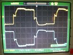
Hi FVM thanks for your reply. My objective is set for discrete parts before gate drive and isolated transformer gate drive. Though it would be tougher this way i still prefer this route than IR ic's and the like due to their cost. If its easier to change those BD to ZTX i prefer to keep things along this route. I will apply Orson's mods, make the measurements and post my results here. I do not have the measurement you were asking but i do have the gate drive transformer secondary waveform and it looks like this: pic3.jpg. Unless I am wrong i think the problem would be around the BD139-140 to the gate turn off transistors. Any help to solve this is greatly welcome thanks
 

It can be seen, that the week primary low side driver (1k resistor) is causing a slow rising edge at the gate. This can be improved by a lower impedance gate driver. The intermediate step in the gate voltae can't be seen at the transformer primary and only partly at the secondary. It seems to be created by the circuit around the gate, which is definitely part of the problem, I think.
 

I will try to disconnect the gate measure the waveform and diconnect the speed turn off and measure the gate transformer secondary to try to sort out the problem and post the waveforms here
 

Hi i've measure the waveforms. This is the GDT secondary unloaded:View attachment ADS00002.BMP

And this is ic signal versus signal at GDT secondary:View attachment ADS00003.BMP

There is no issue with the BD139/140 combination the signal is unaltered after passing through these transistors.

The issue i.e steps in the waveforms is with the GDT transformer but what could be causing this?
 

You see a waveform deviation caused by the magnetizing current and the complentary source follower's voltage drop. E.g. in the middle of the pulse, the current sign is changing, causing a small step and also the assymmetry of the zero voltages.

You either have to change the driver topology, e.g. using a push-pull CMOS structure, as Orson suggested. Or change the secondary circuitry to generate a clean "on/off" gate voltage despite of the transformer waveform.
 

Status
Not open for further replies.

Similar threads

Part and Inventory Search

Welcome to EDABoard.com

Sponsor

Back
Top