cupoftea
Advanced Member level 5
Hi,
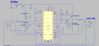
Just downloaded the Synch Buck calculator from ti.com, and for one of their synch buck chips,
i got it to calculate the switching loss. It said top FET switching loss was 2.7W....
NFET CSD18533Q5A was bottom FET
NFET CSD18563Q5A was top FET
Buck was 12.5A out, 13v5 out, 27V5 Vin , 450kHz.
ti.com Synch Buck Switching Loss calculator....
They give the equation for the switching loss, which indeed is the correct one, but that equation does not give 2.7W for switching loss.
It gives less than 0.5 Watt.
I also calculated the switching loss in the manner described in the document by Laszlo Balogh...
..and again, the figure comes out nowhere near 2.7W.
As you know the principle for finding FET_ON switching loss is simple...
..You find the power for two time periods..
1...Time to charge Ciss from Vgs(th) to Vgs(i_pedestal) [i(pedestal) is the "valley" of the inductor current]
2...Time to discharge Cds from Vin to Zero. (Qgd ends up getting used here)
...Both calculations are ultimately from dt = C.dv/i(drive)
where...
i(drive) is the current sourced by the driver, to find which, you need to know the drive output voltage
and the drive series resistance. (And also the "average" gate voltage over the time interval concerned).
-And then its Ohms Law.
Anyway, with the FET_OFF switching loss calculated in the same vain, it comes out as less than 0.5W..
So how did ti.com come up with 2.7W?
Must admit the driver source and sink resistances are low, and i believe on the real product we will have to add series
gate resistance, otherwise the FET will hard-switch too fast, and resulting noise could ruin the operation.
Just downloaded the Synch Buck calculator from ti.com, and for one of their synch buck chips,
i got it to calculate the switching loss. It said top FET switching loss was 2.7W....
NFET CSD18533Q5A was bottom FET
NFET CSD18563Q5A was top FET
Buck was 12.5A out, 13v5 out, 27V5 Vin , 450kHz.
ti.com Synch Buck Switching Loss calculator....
SYNC-BUCK-FET-LOSS-CALC Calculation tool | TI.com
View the TI SYNC-BUCK-FET-LOSS-CALC Calculation tool downloads, description, features and supporting documentation and start designing.
www.ti.com
They give the equation for the switching loss, which indeed is the correct one, but that equation does not give 2.7W for switching loss.
It gives less than 0.5 Watt.
I also calculated the switching loss in the manner described in the document by Laszlo Balogh...
..and again, the figure comes out nowhere near 2.7W.
As you know the principle for finding FET_ON switching loss is simple...
..You find the power for two time periods..
1...Time to charge Ciss from Vgs(th) to Vgs(i_pedestal) [i(pedestal) is the "valley" of the inductor current]
2...Time to discharge Cds from Vin to Zero. (Qgd ends up getting used here)
...Both calculations are ultimately from dt = C.dv/i(drive)
where...
i(drive) is the current sourced by the driver, to find which, you need to know the drive output voltage
and the drive series resistance. (And also the "average" gate voltage over the time interval concerned).
-And then its Ohms Law.
Anyway, with the FET_OFF switching loss calculated in the same vain, it comes out as less than 0.5W..
So how did ti.com come up with 2.7W?
Must admit the driver source and sink resistances are low, and i believe on the real product we will have to add series
gate resistance, otherwise the FET will hard-switch too fast, and resulting noise could ruin the operation.