Continue to Site

Welcome to EDAboard.com

Welcome to our site! EDAboard.com is an international Electronics Discussion Forum focused on EDA software, circuits, schematics, books, theory, papers, asic, pld, 8051, DSP, Network, RF, Analog Design, PCB, Service Manuals... and a whole lot more! To participate you need to register. Registration is free. Click here to register now.

[SOLVED] Suggestion on trigger circuit

Status
Not open for further replies.
In this project, there should be always a current limiting resistor connected in series with the 1 LED or 2.
The only difference in the two cases is that when using 1 LED the resistor value will be higher. And instead of the second LED light, more heat should be dissipated in the current limiting resistor (in my opinion, this is an unnecessary loss).

But perhaps you have just 1 LED (even if you like using 2 LEDs since the battery life will be the same). In this case we will work here with 1 white LED only.

Sorry, I used to verify carefully what I have to work on. It seems you forgot telling me, if your white LED is small or a power one (rated @350mA for example).
 
  • Like
Reactions: kbtan

    kbtan

    Points: 2
    Helpful Answer Positive Rating
Thank You Sir. My LED is the standard (small) 20mA
 

As I mentioned earlier, we can use U4 to drive the LED.

(17) the output of U2 (pin 4) will be connected to one input pin of U4 (say pin 12).
(18) The other U4 input (pin 13) will be connected to Vcc (because U4 is a NAND gate).
(19) Now U4 acts like a simple inverter. If pin 12 is low, pin 11 is high and vice versa.
(20) Since pin 4 will be high for 5 sec then p11 will be low during this time.
.....
Sorry, I forgot asking you if you prefer using an NPN or PNP transistor.
In case of NPN, the load (LED and resistor) will be connected between collector and Vcc.
In case of PNP, the load (LED and resistor) will be connected between collector and ground.

Added:
Perhaps you can tell me the name (label) of the transistor you can use.
 
Last edited:
  • Like
Reactions: kbtan

    kbtan

    Points: 2
    Helpful Answer Positive Rating
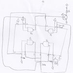
Sir I had draw out the circuit. Can u check whether it is correct.
IMG_20130729_0003.jpg
 

Good work, kbtan.

Your work is correct up to pin 11. After it, as we will see, a PNP transistor should be used. And you missed the resistor before the transistor base (it limits the base current). And I noticed the polarity of the LED is reversed.

First, let us see why a PNP should be used here.

When BP1 is pressed, pin 6 becomes low and the output pin 4 (and pin 12) will be high. This lets the output pin 11 be low (0V). In this case the NPN transistor is turned off (Ib = 0) also the LED, which is the inverse of what we expect. To solve this, we just need to connect pin 12 to pin 3, instead of pin 4 (because, in the flip flop, the state of the two outputs, pin 3 and pin 4, are opposite).

Note: If pin 12 is connected to pin 4 (as we did first), we need a PNP transistor at the output pin 11. Its emitter to Vcc, its base via a resistor to pin 11 and its collector to the anode of the LED which is followed by a resistor to ground. Now when pin 11 is low, the LED is turned on.

Next we will calculate R4 (between pin 11 and the NPN base) and R5 in series with the LED (Don't forget connecting pin 12 to pin 3).
Note: The calculations are the same for the NPN and PNP cases.

First, we need to decide on the LED current. Any suggestion? Please remember the LED is driven by the small 9V battery.
 
Last edited:

OK noted. Sir why a PNP transistor should be used instead of NPN?
 

Please, re-read post #25.

Naturally, the LED current in this project will be less than or equal to 20 mA (though it could be higher than 20 say 30 mA since it is not on always).
Your opinion?

Let us do the calculations in function of I_led_max (the maximum current of LED)


Please ignore below:

===================================================
We also assume the value of the following parameters:

V_sat = 0.2 V (the Vce saturation voltage when Ib is higher than Ic/Beta)
V_led = 3.3 V (the typical forward volatge of a white LED)
Vcc_max = 9.5 V (fresh 9V battery).
Vcc_min = 7 V (used 9V battery).

R5 = (Vcc_max - V_sat - V_led) / I_led_max
R5 is the current limiting resistor in series with the LED
===================================================

The reason is that, in this project, we have excess of volts so V_sat doesn't have to be made too small.
For Vce = 2 V for example the transistor may have an Ic/Ib about 150.
But when Vce = 0.2 V this ratio should be about 20 only, hence Ib should be increased.
 
Last edited:

When BP1 is pressed, pin 6 becomes low and the output pin 4 (and pin 12) will be high
Sir, since pin 4 will be high for 5s when BP1 is press, can i directly connect it to the NPN transistor instead of connected to PNP through U4.
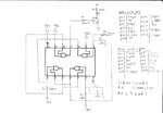
I try to do the calculation. Can u check whether it is correct or not.
IMG_20130729_0005.jpg
 

In theory, connecting the NPN directly to pin 4 is right. But it is always wise not to load, as possible, the flip flop CMOS outputs since they are rather weak sources. As you know pin 4 is already connected to timing RC (via the 330K). This is why I used the remaining U4 as a buffer.

I am reading your calculations.

Added:
Since you assumed Beta=100, Vce should be greater than 1 V.
Let us assume:
Vcc = 9 V
Vce = 2 V
Ic = 20 mA
V_led = 3.3 (a typical value for white and green LEDs)

R5 = ( Vcc - Vce - V_led ) / Ic
R5 = ( 9 - 2 - 3.3 ) / 0.02 = 185 Ohm
R5_real = 180 Ohm

Please note if on the real circuit Vce is less than 2V, it means Beta > 100 (the assumed value).
As a first approximation we assume no drop at the CMOS output, Vout = Vcc = 9V
Ib = Ic / 100 = 20mA/100 = 0.2 mA
R4 = ( Vout - Vbe ) / Ib
R4 = ( 9 - 0.7 ) / 0.2
R4 = 41.5 Kohm
R4_real = 39 Kohm

Extra notes:

(1)
I used the following approximated formula to find R3 and C2:
t (in sec) = 0.693 * R3 (in Ohm) * C2 (in Farad)
This applies when a capacitor is charged from 0 to Vmax/2 or discharged from Vmax to Vmax/2

(2)
You may need adding a small diode in parallel with R3 (330K) to dischage rather quicky C1 (22uF) when pin 4 returns to low after the 5 sec.
 
Last edited:
  • Like
Reactions: kbtan

    kbtan

    Points: 2
    Helpful Answer Positive Rating
Sir, I tried to build the circuit but there are some problem with it.
1) once the switch is press the LED light won go off after 5s. It only go off when i remove C2 connection to ground.
2) I am using HEF4093BP NAND GATE instead of using CD4011. Is it compulsary to use CD4011???
3) The battery supply 7.96v.
4) I am using TIP31a npn transistor
Is it the 2 and 3 cuz the circuit didn't work properly???

Below show my circuit and reading measured
IMG_20130730_00081.jpg
 

You did well in building the circuit. Since it failed, this means we will learn new things.
For instance, I have, most of the time, learnt better how to design electronic circuits... from my continuous failures during the last 40 years ;)

Using 4093 could be used, but its inputs draw much more current than of 4011 when its voltage is between low and high state (see datasheet).
So the high value resistors we used for 4011 don't work here. As you saw, pin 6 is 5.43 V (before switch press) while it should be close to Vcc.

Although it is much better using 4011 for your project, here are the changes we will do if 4093 is used on the previous circuit:

(1) R1 is removed since pin 1 is connected directly to an output (pin 10). Note: This also applies for 4011.
(2) R2 = 3K3
(3) C1 = 100nF
(4) R3 = 2K2
(5) C2 = 1000uF (This is an estimated value since the previous formula of 't' doesn't work. During the charge, the output voltage at pin 4 and the input current at pin 8 are no more constant and neglibible).

Notes:
(1) During your tests, you can use R5 = 1.8 Kohm instead of 180 Ohm, to save the battery power.
(2) Since 4093 specifications may differ from one manufacturer to another, you can experiment higher values for R2 and R3, hence lower values for C1 and C2.

About your notes on your drawing:
I noticed you wrote R5 (24mA, 3.3 V). But 0.18 * 24 = 4.32 V
Also you wrote R4 (9.5 mA). But 39 * 9.5 = 370.5 V
 

I noticed you wrote R5 (24mA, 3.3 V). But 0.18 * 24 = 4.32 V
Also you wrote R4 (9.5 mA). But 39 * 9.5 = 370.5 V

Sorry Sir.I think 3.3V is for the LED.
for R4 , i touch the R4 resistor with the multimeter, it give out such reading

Sir in post 29
(2)You may need adding a small diode in parallel with R3 (330K) to dischage rather quicky C1 (22uF) when pin 4 returns to low after the 5 sec.
is it neccessary to put the diode??. I try put the diode parallel to it with the anode(no strip) facing toward pin 4 . When I press the switch the LED will blink. in oposite direction, the result is same as not puting the diode
 

If you measure the voltage on R4 (V_r4), Ib = V_r4 / R4.
If you like to measure Ib directly, the ampermeter will be connected in series with R4 (not in parallel, since its internal resistance is close to 0 Ohm).

About the diode, if its anode is at pin 4, pin 4 will charge C2 via the diode, not R3. So C2 will be charged quickly and, as you said, the LED will likely blink.
For the reverse direction, the LED on-time won't change. But the reversed diode helps to faster disharge the capacitor C2 and let C2 be ready for another cycle in a shorter time, otherwise C2 will have to discharge rather slowly via R3.
 
  • Like
Reactions: kbtan

    kbtan

    Points: 2
    Helpful Answer Positive Rating
Hi kbtan,
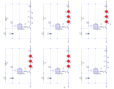
By using 555 timer in Astable mode it is possible to make trigger circuits.
Have a look to my circuit below, it is designed for 5 Sec and suited for your requirements.

This is an animated circuit.
555 Monostable Edaboard.gif

When I trigger the circuit, the LEDs glows up to 5 Sec and returns to OFF state.
Still confused please share your problems here.
 

Status
Not open for further replies.

Part and Inventory Search

Welcome to EDABoard.com

Sponsor

Back
Top