R.Maher
Newbie

Hello everyone,
I try to design an RF rectifier using ADS co-simulation. I am confused about the correct definition of the substrate.
I need to define the back side of the substrate as the ground. what is the correct way?
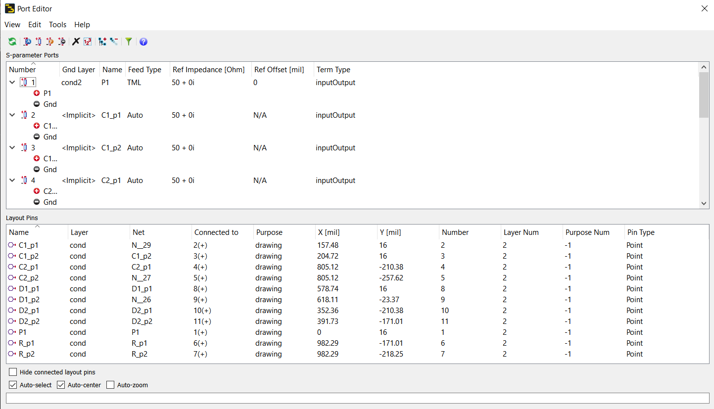
I defined two copper layers (on top and bottom of the dielectric), draw my layout on the top layer, draw a rectangular shape on the back side, and define this back conductor as the ground for the input port.
I used TML calibration for this input pin port only.
Are these steps correct to match measurements?
Also If get negative real impedance from the layout EM simulation (before connecting lumped elements for co-simulation),
What does this mean?
Thank you all and waiting for your help.


