Continue to Site

Welcome to EDAboard.com

Welcome to our site! EDAboard.com is an international Electronics Discussion Forum focused on EDA software, circuits, schematics, books, theory, papers, asic, pld, 8051, DSP, Network, RF, Analog Design, PCB, Service Manuals... and a whole lot more! To participate you need to register. Registration is free. Click here to register now.

[SOLVED] Stability Simulation with Cadence

Status
Not open for further replies.
Dear frank,

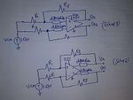
in the pdf Idaho he changed the place of the difstbprobe when he was simulating the CMFB loop however he was using cmdmprobe as I am again reffereing to it below.

But I would also get confirmed about your suggestion more clearly, according to you that the same circuit configuration used to simulate the differential mode properties using the diffstbstbprobe will be exactly the same to be used for simulating the common mode CMFB loop proparties but by only changing the STB setting from the simulator from differential to common,

the setup I am again bringing it near to you here

idaho.jpg

444.jpg
 

If you have more CMFB loops you could test them separately, but you mentioned only one loop. To test that I think you don't need to move the probe to an other place.
Why don't you try it and compare what happens if you move it?
 
Dear Frank, i will simulate every type and I will put the result after each one

so here first the result of the CMFB loop stability test.

I used the setup 1 from the image above,
Then I changed the stability simulation setting to ''Common'',

Result are shown below, which is I think I am getting it inversely

CMFB1.png

CMFB11.png

- - - Updated - - -

*****************************************************************************************************************
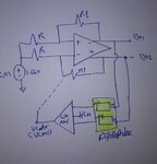
below is the simulation of the CMFB by using the setup below using the Iprobe,

setup.jpg

CMFB22.png

CMFB2.png
 

Attachments

  • CMFB2.png
    CMFB2.png
    65.3 KB · Views: 363
Last edited:

Looks like you don't have any phase margin in your CMFB, if i correctly understand your plots. Is that right?

By the way, when I asked you about the polarity of the main amplifier stages in common mode, I didn't mean how the CMFB amplifier works. What I meant was that you have your 1st amplifier stage (the folded cascode) connected to the output stage. And it was interesting for you to figure out what was the polarity (inverting or non inverting) of these two stages for common mode.


- - - Updated - - -

In the general case, yes. In simple case e.g. the discussed CMFB loop, you get away with voltage transfer function only https://www.edaboard.com/showthread...plifier-loop&p=1643117&viewfull=1#post1643117

FvM, I would agree that Middlebrook's method can go simply with a voltage source at the loop break point when the impedance looking into the stimulated point is much higher than the one at the return point. This assumption breaks at high frequencies where most of the time we care about the response.
 
Dear Suta

This is I cant understand even, the graph is showing that I have no phase margin but it is technically impossible, because I am running the AC simulation in my circuit and I am not getting oscillation. I don't know what to talk about the result.

the right output is non inverting and the lift one is inverting,
-----------------------------------------------------------------------------------------------------------------
by the way Suta, I asked about the differential gain I got before performing the CMFB loop gain, is the gain I get by the diffstbProbe is (Vo1-Vo2)/(vin+ - Vin-) or it is related to the one of the single outputs

- - - Updated - - -

+++++++++++++++++++++++++++++++++++++++++++++++++++++++++++++++++++++++++++++++++++++++++++++++++++++++++


Dear friends here I came with the last setup,

here I used the diffstbProbe as in the attached method and by changing the STB setting to Common instead of Differential , result are full matched to the method by using only Iprobe.

CMFB3.png

CMFB33.png

jun.jpg

if you look to the graph not to the result summary you will see that I have a lot of phase margin...

- - - Updated - - -

another way I look in to the stability is by looking at the nearest coming pole,,, can you please see that the next pole (next bend in the loop gain graph) is far away from the point of 0dB which confirm the stability
 

I don't know what can I say about my graph, i it stable or not please, is there other way to get confirmed
thank you
 

The CMFB loop gain plots look consistent at first sight, indicating the lack of a dominant pole. It should also show by heavy ringing (or oscillations) in the closed loop response.
 
Dear FvM,

Thank you very much for your reply

I am simulating the circuit in time domain but I am not oscillating. I am applying differential sin signal under closed loop and running the transient, every thing seems ok..

But may be you mean to say by other kind of transient simulation which can see the stability of the CMFB..

the other thing FvM as you said the response itself is also not clear, the dominant pole is not located at low frequency.
 

Don't apply sine signal to your amplifier. Keep the inputs at the input common mode voltage. Under these conditions you should inject some disturbance in the common mode loop and see how the circuit settles. For example attach a pulse or pwl current source between Vcntrl and ground. It starts with a value of 0 in the beginning and at some time give it a pulse of current - maybe 1/4 or 1/2 of the current you have in your CMFB amplifier output stage. Keep the current at this value for some time, then drop it again to 0. See how the circuit behaves.

Next, start your transient simulation with supply at 0v and then ramp it up to its value. See if the circuit starts up properly.

Then do one more experiment - with regards to your transistor level schematic, keep Vbias7 high at supply (short it with some switch, for example) while the supply is ramping up. Your schematic will not be functional in this case. Keep Vbias7 at supply for some time until everything settles and then let it go to its intended value by turning off the shorting switch. See again how the circuit behaves.
 
Dear Suta,

I applied a small pulse signal to the VCM terminal of the common sense amplifier (CMFB amplifier) above the DC voltage of 1.65 V. I run the circuit while the circuit inputs are at the common mode voltage with closed loop condition, I run the transient simulation and the circuit is giving me oscillation at the output (viabrating from 3.3 to 0).

is it correct setup or not ?
 

Differential gain expression using the stability analyses for testing fully op-amp

Dear friends,

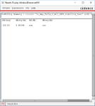
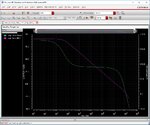
So far I have successfully simulated the AC characteristics of my differential amplifier using the diffstbProbe in cadence as shown below,

I can see my closed loop gain gain from direct plot as also given below,
as you can see the DC gain is 90 dB.

I have one question regarding this result please:

is this the gain of the expression (Vo1-Vo2)/(vin+ - Vin-) ?..... case one

or this represent the gain of Vo1 / ( (vin+ - Vin-) = Vo2 / ( (vin+ - Vin-) ?..... case two

444.jpg
difresult.jpg

Thank you very much in advance
 

Re: Differential gain expression using the stability analyses for testing fully op-am

Is this the gain of the expression (Vo1-Vo2)/(vin+ - Vin-) ?..... case one

Yes, this one.
 

Thank you Vive, now it is very easy to simulate the AC
 

Dear friends,

I came to compensate the CMFB loop by reducing the gain of my common sense amplifier, such reduction I didn't expect to do because I am using diode load connected differential amplifier controlling fraction of the CMFB control voltage, it means basically my CMFB amplifier gain is less than one, however the loop gain is so high that I was loosing the stability.

I would like to thank you so much for supporting me in this issue.
 

Dear Suta,

I applied a small pulse signal to the VCM terminal of the common sense amplifier (CMFB amplifier) above the DC voltage of 1.65 V. I run the circuit while the circuit inputs are at the common mode voltage with closed loop condition, I run the transient simulation and the circuit is giving me oscillation at the output (viabrating from 3.3 to 0).

is it correct setup or not ?

Applying a pulse at VCM is not quite what I meant. This way you're testing the step response (for long enough pulse) of the closed loop. What I meant was for you to test the step response of the loop itself by injecting that pulse inside the loop.
 

Applying a pulse at VCM is not quite what I meant. This way you're testing the step response (for long enough pulse) of the closed loop. What I meant was for you to test the step response of the loop itself by injecting that pulse inside the loop.

If you want to assess the CMFB loop stability, both test setups can be expected to have quite similar result.
 

Yes FvM that is right, if we apply the step to the VCM input of the error amplifier or if you introduced either in some where in the loop both will have the same effect,

Before I compensated my loop and when I applied te step signal at the VCM the amplifier was vibrating, now I repeated the same simulation after compensation and the amplifier is stable.

I read now more about the stability of the loop feedback and every literature is assuming that if my error amplifier gain is less than or equal to one the CMFB should be naturally stable, then why it is not the case of my design?

The thing is that when I reduced the gain further, the error of the output VCM is increased, now I have about 30mV error from 1.65 V.

Thank you very much
 

Actually, I don't agree much with the above. If you put a step at VCM you're testing the response of the closed loop CMFB system. Otherwise, with step in the loop, you see how the loop gain reacts, because it is supposed that in this case the VCM stays fixed. But, practically, it doesn't really matter in this case if the loop is unstable.

It is also expected that reducing the gain of the CMFB error amplifier will increase the error between the actual CM voltage and VCM. You reduce the loop gain T and this error is proportional to 1/T.
 

Dear suta,

Surely when reducing the gain of the error amplifier the error of the output VCM, but i have no other option, I tried to use compensation capacitor but it is not working with me, I connected it by different places but I don't know why it is not working,

if you think of good compensation scheme then your suggestion will be welcomed.

Now Suta I come to your argument about the step response, actually the step response is also a method of testing stability, like in an amplifier when you apply a step at the input then from the output you can expect the stability
 

For a specific feedback topology, loop gain and closed loop gain are clearly related. In most feedback amplifier applications, closed loop behaviour is the property of interest. It's often possible to assess the system performance sufficiently by testing the closed loop response. E.g. if the step response of a single loop feedback system doesn't show oscillations, you know that it has sufficient phase margin.

Analysing the loop gain gives nevertheless additional information, particularly if you want to improve the stability.
 

Status
Not open for further replies.

Part and Inventory Search

Welcome to EDABoard.com

Sponsor

Back
Top