Continue to Site

Welcome to EDAboard.com

Welcome to our site! EDAboard.com is an international Electronics Discussion Forum focused on EDA software, circuits, schematics, books, theory, papers, asic, pld, 8051, DSP, Network, RF, Analog Design, PCB, Service Manuals... and a whole lot more! To participate you need to register. Registration is free. Click here to register now.

SPI Slave with strange behavior

Status
Not open for further replies.

rmachado

Member level 2
Member level 2
Joined
Apr 13, 2018
Messages
45
Helped
0
Reputation
0
Reaction score
1
Trophy points
6
Activity points
668
Hi everyone,

I don't really know if this is the right place to do this post, so if it is not, please redirect me to the right place.

With that being said, let me explain the problem I am working on right now.

Some time ago someone in the company at which I am currently doing my PhD developed an ASIC with an analog and digital part. The analog part is responsible for doing some measurements and the digital one is composed by an SPI slave, a register bank, that has the registers responsible for configuring the entire ASIC, and some other components that are not relevant for the problem at hand.

The design passed all the functional and timing verification and they tape-off the chip for manufacturing. When the ASIC chip was ready, they find out that the SPI Slave communication was not working properly. Most of the masters that they use to communicate with the slave are not able to write to it, and the one that works, the MCP2210, only writes to it sometimes and most of the times when they use it to read from the slave, the values are wrong. As I am doing my PhD in the ASIC design field, they ask me if I could look into the problem but right now I am at a dead end. So I hope that someone here can give me at least some hints on what tests should I do next and what kind of stuff should I search for.

Here is what I have done so far:
1- I run the functional and timing tests again just to double check the validation process and to look at the communication waveforms and timings. As I was expecting, the ASIC passed the test.
2- Looking into the problem, I guessed that the problem could be related with the SPI slavve or the writing/reading from the register bank so I picked that code and implemented it in a ZYBO FPGA (I know that the hardware result from this implementation is completely different from the real ASIC, nevertheless I decided to do it using the same constraints file just to see if I could get a similar behavior. Some time ago I discovered a reset problem in a I2C ASIC by adopting this process). The FPGA system works perfectly as expected. no matter the master SPI device I use, being it the aardvark, mcp2210, or even the arduino zero board, the communication between the SPI masters and the FPGA SPI slave works perfectly, even at the maximum SPI Master clock frequencies.
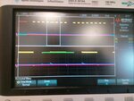
3- I monitored all the tests using an oscilloscope with probes for the Sclk, MISO, MOSI and CS signals. The master generates all the signals correctly but the slave just simply does not respond on the MISO line (I attached a picture with the waveforms from the oscilloscope, although i don't believe that it will help a lot).

I check the SPI mode as well and I know both master and slave are in the same operation mode (in this case, mode 0 CPOL=0 and CPHA=0)

Clearly, the verilog code is functionally correct, otherwise the design would not work on the FPGA. So there must be something on the ASIC chip behind the failure but i can not understand what is it. maybe the pads? right now I am out of ideas.

So can anyone give me some hints on what could be causing the problem to appear on the ASIC but not in the FPGA? And does anyone have some test ideas for me to perform so I could dig deeper into the problem?

Thanks in advanced,

Rui


IMG_20180608_145828[1].jpg
 

Hi,

Please give detailed informations about the problem:
* informations about test setup, like hardware, frequencies, voltage levels...
* give informations what you expect. Like a picture of the waveform that you exoect...
* give infirmations about the wrong result. Like the scope picture, but with informations where you see the problem.

By viewing to your scope picture, the problem can be:
* signal ringing
* bad GND connections
* wrong voltage levels
* ...

Klaus
 

There's definitely too little information to guess substantiated about the SPI failure. The fact that it's working at times with the MCP2210 interface should allow you to narrow down the problem, probably by using a fully programmable master source, e.g. a multichannel arbitrary waveform generator. You should take into account all signal parameters like frequency, timing, logic level, rise- and fall time.

Your oscilloscope screen shot seems to show a tri-stated MISO line (according to the SCK cross talk). Is this by design? When will the MISO driver be activated in normal operation?

The observation that the slave design works in FPGA but not in ASIC could also indicate a bad timing design, depending on the topology.

I presume there's no testability built into your ASIC, e.g. boundary scan functions?
 

Sorry for not being completely explicit on the first post.

Regarding the test setup I have the master SPI device (I did the test with both the SPI from arduino zero and the mcp2210) connected to my slave device (the FPGA in one test, and the ASIC chip in a separated test). All grounds are shorted to ensure a common ground and then the SCLK, MISO, MOSI, and CS pins are connected between the master and the slave, all these signals are being monitored using the oscilloscope. I try using 8MHz, 4MH, 1Mhz and lower clock frequencies for the SCLK, all of them work on FPGA, none of them worked on the ASIC. I am working with 3.3V in all devices, the master device supply source is from my Host computer via an USB cable, while the slave device supply source is a power supply from keysigh regulated at 3.3V (when the slave is the ASIC chip), or the host computer via a USB cable (when the slave is the FPGA) .
Regarding the expected results, after the first clock group, in which I send to the slave the register address i want to read, I was expecting the MISO to had the value on that register, instead, the slave returns always zero and I know that the register I am reading have a different value.
I guess I could implement a master SPI by software using bitbang on arduino zero, so i can test the ASIC ate very low frequency ranges and then, if it works, slowly increase the frequency to try to figure out at which point the device is failing. That should point me if it is indeed a design timing issue.

Regarding the tri-state MISO line, as far as I know, it is not by design, I don't know if it is possible to do it depending on the type of pads, but I also don't know which type of pads did they use on the Chip, I only have the HDL code, I will ask them. When I first saw the MISO line I also found it strange.

Regarding the testability of the ASIC, you are right, they do not add any scan chains to it.

I will start by implementing the bitbang SPI at very low frequencies and once I haave the results I will post them here.

If you need more info just let me know and thanks for your time.
 

Regarding the tri-state MISO line, as far as I know, it is not by design, I don't know if it is possible to do it depending on the type of pads, but I also don't know which type of pads did they use on the Chip, I only have the HDL code, I will ask them. When I first saw the MISO line I also found it strange.

The expectable behavior should be obvious from the HDL code. Popular options are:
- using nCS as unconditional enable
- enabling MISO conditionally after a read command has been received, accounting for optional common MOSI/MISO line

Depending on the option implemented in your HDL you can further conclude about the nature of failure.
 

Here is what I figured out regarding the HDL implementation.

The CS line is used as an asynchronous reset for the SPI. When a rise edge on the CS line occurs the Chip enters reset and stays there until the CS line is force to zero again. For the slave to work in the normal mode the CS line has to be at logic level zero. The CS line does not have a direct influence on the output of the MISO line.
Regarding the MISO line, the slave can work in two modes but if the command sent to the slave is not a read command the line is forced to low, otherwise the MSB from the shift register is passed. Something like :

assign MISO = (mode ? dataOutRegMode1[7] : dataOutRegMode0[7]) && ~cmd[0];

So cmd[0] is working as an enable for the MISO line. Could this be the origin of the problem? I can't understand why?

I noticed that the cmd[0] signal is also used in some always blocks to enable the loading of the value to send to the shift register or to enable the sampling of data from the MOSI line.
 

Hi,

U
The CS line does not have a direct influence on the output of the MISO line.
Usually the CS line should control the ENABLE of the MISO driver.
CSn = 0 --> driver enabled
CSn = 1 --> driver disabled

Klaus
 

In the implementation they have, the CS control the reset of the SPI together with the system reset signal, and the MISO is enabled or disabled using the write/read bit, given by the cmd[0] register. if the CS line is equal to 1, the SPI is in reset mode which means cmd is cleared and cmd[0] = 0, which means the MISO line enabled.... with CS = 0 the cmd register is equal to the last command received by the slave, if it is a read command the MISO continues enabled, as the cmd[0] = 0, if it is a write, the cmd[0] = 1 and the MISO line is disabled (pulled low).
This works fine in the FPGA. I don't know if this is the cause of failure in the ASIC chip, but if it is, how can I be sure of it, I can not think in a test that would give me the answer to that.

I can agree with you that the design they implemented is not the best, nevertheless i can not change the ASIC they already fabricated, I just have to try to find the reason of failure so then we can think on a fix.

Thanks,

Rui
 

So I did a bit bang master SPI code on arduino zero to test the slave at low frequencies.
I started with a clock period of 4ms (250Hz) which I consider low enough.
To make sure the code was correctly done I test it using the slave on the FPGA. Everything worked perfectly.
After that I connect the zero board to the ASIC chip and stated to send data to it and then check if I was able to read that that back. I had no success. Even at this frequency range I was not able to successfully write or read from the Slave, so I am guessing that this might not be a timing issue.
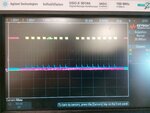
I have attached two oscilloscope waveforms in which I am sending the address 0x04 with an order to read (LSB = 0). I am expecting a 0xa6 value from the slave but the MISO line do not respond, returning the value zero.

IMG_20180611_111804.jpgIMG_20180611_111742.jpg
 

Hi,

which color (channel) is what SPI line?

Klaus

Added:
I assume
yellow = SCK
if so, where is the 9th clock for ACK?

Klaus
 

sory I forgot to legend the images.

Yellow is clock (there are only 8 clocks per transmission, only 16 pulses if you count on the image)
Green is MOSI
Blue is MISO
Pink is CS

first 8 pulses are the address + write/read bit -> to read from address 4 i have to send via MOSI 000_0100 + 0
then the following 8 pulses are given so that the slave can write to the MISO, but instead of having the value presented on the register that has the address 4 I am having only zeros.
 

Hi,

Added:
I assume
yellow = SCK
if so, where is the 9th clock for ACK?
Sorry, I confused this with I2C...

Klaus

- - - Updated - - -

Hi,

In opposite to I2C here with SPI the data_out should be aligned with one clock edge and the data_in with the opposite clock edge.
(With I2C the output is at a low phase - like in your diagram).

This doesn´t mean that your implementaion is wrong, but it reduces the timing margin.
Are you sure both - master and slave - are designed to operate with CPOL = 0 and CPHA = 0? Usually you can' t decide this on your own but need use the (one) suitable solution.

I assume your scope screenshots are with the ASIC.
--> Then show use the same communication with the FPGA

Klaus
 

the screen shots are with the ASIC. with the FPGA I dont even need to check the wavefoms cause i am able to write and read the values from the registers correctly.
The slave was developed to work at mode zero (CPOL and PHA equal to zero).
I did the data change at the middle of the low level on purpose to make sure that there was not some strange behavior on the side of the slave at the fall edge transition, as the slave is sampling the data on the rise edge of the SCLK, I don't think there is a problem in doing this. I changed the bitbang master code by removing the delay I am adding after the fall edge and test it again and the result were the same.
 

Hi,

with the FPGA I dont even need to check the wavefoms cause i am able to write and read the values from the registers correctly.
Then we are not able to cross check behaviour and see possible differences.
I did the data change at the middle of the low level on purpose to make sure that there was not some strange behavior on the side of the slave at the fall edge transition, as the slave is sampling the data on the rise edge of the SCLK, I don't think there is a problem in doing this.
As said: It won´t be a problem here with low SPI clock.

If you send out the data at the middle of the low phase
and it´s sample on the rising edge.

Then it has only 25% of a clock cycle time to stabilize and 75% are useless.
If you really want to relax timing the you should go the other direction and send out data in the middle of the clock high phase before.
Then it has 75% of time to stabilize ... and a hold time of 25% of a clock cycle.

Klaus
 

You are right regarding the time relaxation, I will do a test with it right away. I will also record the FPGA signals and post them in my next post.
I am also having a meeting in a few minutes to discuss the SPI issues so maybe I will get some more ideas regarding the origin of the misbehavior of the SPI.
 

Hi,

As said: It won´t be a problem here with low SPI clock.
No, don't waste your time with modifying MOSI timing. This won´t cause the problem.

Klaus
 

Could the problem be related with cross talk between the SCLK and the MISO line?
I went back to the first image that I post and it is really strange the behavior of the MISO line every time the SCLK has a rise transition. Even in the low frequency SCLK test, the last image I post, a 500mV spike is noticeable on the MISO line at the clock rise transitions.
The company decided to bound some extra chips in a different way so I could test them. I will be waiting for them to deliver me the chips and will run the tests again to see if the problem is or not related with the bounding process.

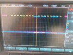
As I promised, I attached the FPGA test waveform just for comparison with the ASIC waveform. The result is the read value from address 4 after I write the value 0xa6 to the register. As it is possible to see, the value return in the MISO line (Blue signal) is correct and also the MISO line does not present the spikes that appear on the ASIC waveforms every time the clock line goes high.

IMG_20180611_160248.jpgIMG_20180611_160310.jpg
 

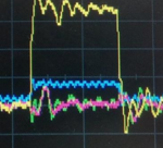
Given the following two pictures showing what I'm assuming is the MISO line in blue for both. The output driver of the ASIC is shorted with something or there is something wrong with the output cell used.
Capture1.PNG
blue "attempts" to go high only during the high phase of the SCLK.
Capture.PNG
Strange "runt" pulses on the leading edge of the SCLK.

Both of these behaviors are very suspicious.

- - - Updated - - -

Ah, I see with your update you noticed both of these issues.

The new set of images from the FPGA code look very good, so you may be on to something with the bonding out of the die being a problem. Maybe the bond wire for the MISO line crosses over with a ground wire and the are shorted. The "The company decided to bound some extra chips in a different way so I could test them" is merely not attaching that crossed ground. I'm sure you won't be able to get them to tell you that if they screwed up the layout.

- - - Updated - - -

BTW, I pointed out the ground wire possibility, because if you later get new parts and they later exhibit weird grounding issues, it might be good to remember that maybe they left off a ground connection to "fix" (really hide) the problem you are currently experiencing.
 

I can not reveal the name of the people I am working with, they allow me to investigate and search for help on my own but with some restrictions (like I can not show the code to anyone and I can not reveal the company identity).
I don't really know what they will do differently in the bounding process, they just tell me in a meeting this afternoon, after I share with them my conclusions and results, that they will do two or three more chips bounded more carefully for me to test. As soon as I get my hands on them I will test them and share with you my results.
 

Hi,

use an external pullup (about 2k2 ... 10k) at the MISO and see what happens.

***
Now the MISO seems to be pulled to GND -- all the time.
But the MISO needs to be HIGH IMPEDANCE all the time when CS=1
(and it should be low impedance when CS=0 all the time; either driven LOW or driven HIGH)

With the pullup test you might be able to detect if the MISO wiring is correct at all.

Klaus
 

Status
Not open for further replies.

Part and Inventory Search

Welcome to EDABoard.com

Sponsor

Back
Top