Continue to Site

Welcome to EDAboard.com

Welcome to our site! EDAboard.com is an international Electronics Discussion Forum focused on EDA software, circuits, schematics, books, theory, papers, asic, pld, 8051, DSP, Network, RF, Analog Design, PCB, Service Manuals... and a whole lot more! To participate you need to register. Registration is free. Click here to register now.

[SOLVED] SMA-Microstrip transition removal for large-signal measurement of PA

Status
Not open for further replies.
But once again, is it really serious at 2.4 GHz?

You can add a few nH in simulation and test it. The photo was for the matching circuit input, which is not a 50 Ohm environment. If it is low impedance, inductance matters more than for a high impedance point.

I still don't understand your design workflow, and if/how an error in measured matching circuit (only that, not full circuit) would affect the final circuit.
 

Hi,

And I wonder where the problem is to post the requested back side.

I'm no HF guru, but what I've learned so far is, that - especially with HF - the GND plane is as important as the signal routing side.
Every HF traveling on the one side causes HF to travel on the GND plane back..at almost the same location as on the signal side.
A cut in the GND plane avoids this, the signal back needs to travel elsewhere..causing a jump in characteristic impedance.

Thus my limited HF knowledge is the same as BigBoss says:
But GND GND GND.. this is important.

Klaus
 

Hi all,

Thanks a lot for your time and kind considerations of my issue.

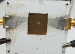
Attachment is the backside of my PCB. I used a buffer thin aluminum plate to make ground connection for SMA connector since the substrate height is just 0.75 mm.
The square cutout in the aluminum plate is at the transistor place to make heat flow. I made measurement of my PCB in both case of w/ and w/o this cutout but the results were similar. I still lost nearly 3dB of output power leading to gain and PAE and drain current drop.

Regarding your recommendations, I am going to try the following solutions:
+ Use another high quality SMA connector with a aluminum base as suggested by @BigBoss
+ Reduce air gap at the SMA connector to PCB; run a simulation to check imperfect connector mount as suggested by @FvM
+ To @volker@muehlhaus: My photo is output matching circuit not input and for 50 Ohm environment. My design workflow is as follow: running a load/source pull simulation in ADS using a large-signal model from Qorvo to find optimum load/source impedances at f0, 2f0 and 3f0. I didn't use impedances given in the datasheet of the device. After this phase, I designed input and output matching circuits using microstrip lines on a RO4350B substrate to check if they could realize these impedances and their losses. I compared measured impedances with simulated impedances and I found that when I used port-extension simulated impedances agreed well with measured impedances (shown in the photos of Smith chart I already posted).
However in the large-signal measurements for output power, gain and PAE for the final PCB, port-extension cannot be applicable (it is just used for S-parameter measurement). This makes me think that the measured output power drop is caused by some phase shift somewhere in the final PCB.
+ To @KlausST: Thank you. I think I will re-check my ground connection at the SMA connector as well as the ground plane.

I will appreciate all of your further considerations of my issue.

20200324_150646.jpg
 

+ To @volker@muehlhaus: My photo is output matching circuit not input and for 50 Ohm environment.

Sure, but you misunderstood me. You need a matching circuit because the transistor side impedance is not 50 Ohm, and that is where your gap creates the extra inductance in the matching circuit PCB.

I compared measured impedances with simulated impedances and I found that when I used port-extension simulated impedances agreed well with measured impedances (shown in the photos of Smith chart I already posted).

I see ... then you might be lucky. If simulated and measured agree (after phase offset), maybe the bad transition doesn't make that much difference.

Did you check the amount of phase offset (i.e. create a short at the circuit input to verify you have the correct phase offset)? Or did you just add "arbitrary" offset until the curves agree? Arbitrary offset might hide/compensate parasitics to some extent.

However in the large-signal measurements for output power, gain and PAE for the final PCB, port-extension cannot be applicable (it is just used for S-parameter measurement). This makes me think that the measured output power drop is caused by some phase shift somewhere in the final PCB.

But phase shift in a 50 Ohm system doesn't make any difference to the load seen by your PA. Only if the coax-to-PCB transition creates a mismatch this would have an effect. Mismatch or not? Looking at your photo, OI would say: yes, mismatch. But you just described that the mismatch in the separate "matching circuit testcase" disappeared. Hmmmm ....

And of course, there can be differences/mistakes in your active devide model simulation. That is more sensitive to errors than passive devide modelling...

~~

Your ground connection is even worse than expected. Don't expect any useful data with such a test setup. Replace the aluminium place by local copper pieces at the connectors, and create a good AS SHORT AS POSSIBLE PATH connection from connector body to PCB backside. Don't just use the pins, you can solder to the outer body of the connector. Remember, 1mm too much length in that path is ~1nH extra inductance.
 
Last edited:
  • Like
Reactions: ueckid

    ueckid

    Points: 2
    Helpful Answer Positive Rating
Now I have seen the problem..As I said before.. GND connection is too poor.
 
  • Like
Reactions: ueckid

    ueckid

    Points: 2
    Helpful Answer Positive Rating
Status
Not open for further replies.

Part and Inventory Search

Welcome to EDABoard.com

Sponsor

Back
Top