Continue to Site

Welcome to EDAboard.com

Welcome to our site! EDAboard.com is an international Electronics Discussion Forum focused on EDA software, circuits, schematics, books, theory, papers, asic, pld, 8051, DSP, Network, RF, Analog Design, PCB, Service Manuals... and a whole lot more! To participate you need to register. Registration is free. Click here to register now.

SMA Connector - Not work - Is there any way to solve it?

Status
Not open for further replies.

imtiaz369

Member level 2
Member level 2
Joined
Jul 8, 2021
Messages
45
Helped
0
Reputation
0
Reaction score
0
Trophy points
6
Visit site
Activity points
488
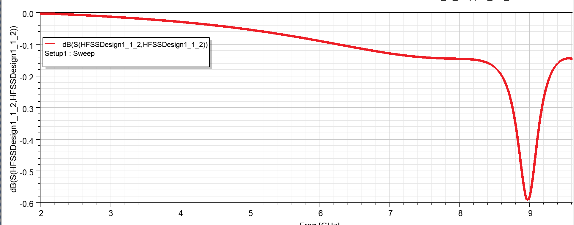
When I used an SMA connector instead of a hfss port (lumped/wave), it returned an incorrect s11 (see attached image). Everything is fine because the pin is properly connected to the antenna's feed line.


But why it is showing this type of behavior?

Are there any additional things need to do when I try with a SMA Connector model?


1701711971656.png

1701712008616.png
 

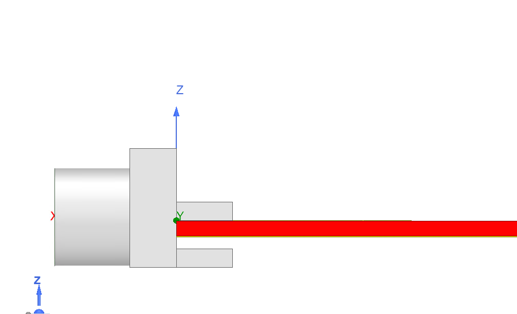
According to post #7 graph, two ports seem to be present, but I can't recognize them on #13 images, neither position nor connection.

It's also not clear what's the significance of post #15 plot.
 

It's still not clear if the simulation has one or two ports. If two, can you show the plot for S21?

If it's just one port, then have you put some sort of terminator on the other end of the line? If not, then your S11 plots look as expected.
 

But of course, the "normal" testcase for a line is to place ports at both ends.
I agree with this, specifically, wave ports in HFSS which will automatically provide the correct termination impedance.

What I meant here is a method to make sure that all signals at the end of the line are absorbed, regardless of line impedance. This can be achieved by running the line straight into a PML wall (no distance!). One situation where this is used in simulation is "measurement" of line impedance, input impedance at the port is then equal to line impedance because there is never any reflection from the PML side.
I have doubts about this, although I've never tried it and no longer have access to HFSS. The PML would be contacting three different materials (substrate, air, conductor) - how would its properties be set? :unsure:
 

That is a different case: for antennas we place absorbing PML boundaries at some distance, with airbox between antenna and absorbing boundary.

What I meant here is a method to make sure that all signals at the end of the line are absorbed, regardless of line impedance. This can be achieved by running the line straight into a PML wall (no distance!). One situation where this is used in simulation is "measurement" of line impedance, input impedance at the port is then equal to line impedance because there is never any reflection from the PML side.

But of course, the "normal" testcase for a line is to place ports at both ends.

Thank. I used a PML boundary now instead of a regular radiation one. However, the problem is still showing. It's an antenna simulation, where I want to see a real measurement scenario in the simulation.

By the way, in the case of the transmission line, when I used sma in both ports, the S11 looked fine, as expected.

So, the SMA design is correct, at least okay for the simulation.

Well, But now I just want to use one SMA -- so after that, it is now working at all, without PML. Are there any other things I need to do for One port SMA Connectionb>
 

Ok, so the antenna doesn't work as expected, but the through line works.

Why do you think the issue is the sma/port feed, and not the antenna itself? Have you tested your antenna model with another port type?
Without sma, it is working fine. I want to see the response with SMA.
 

Without sma, it is working fine. I want to see the response with SMA.
Apparently some basic fault or misunderstanding about port connection. Without seeing the design details, we can only guess.

A coaxial connector acts like a short piece of transmission line. Both sides needs to connect center pin and ground, otherwise an open circuit is created.
 

I don't have HFSS experience but why there are some "unusual boundaries" underneath of the MS Line and GND ?? Is it normal ??
I have also seen in some examples, HFSS Hybrid Mode solution type is selected in similar problems, does it make sense ??

1702544215323.png


1702544230789.png
 

Get some information from hfss animation plot. You will come to know if RF signal is able to reach the microstrip through SMA connector or getting reflected back at connector itself. The RF signal is suppose to travel to the other end of the microstrip.
 

Status
Not open for further replies.

Part and Inventory Search

Welcome to EDABoard.com

Sponsor

Back
Top