Continue to Site

Welcome to EDAboard.com

Welcome to our site! EDAboard.com is an international Electronics Discussion Forum focused on EDA software, circuits, schematics, books, theory, papers, asic, pld, 8051, DSP, Network, RF, Analog Design, PCB, Service Manuals... and a whole lot more! To participate you need to register. Registration is free. Click here to register now.

[SOLVED] Reverse polarity detection (I need an idea)

Status
Not open for further replies.
I omitted the rest of the circuit in order not to confuse things. The diode is in fact a part of boost converter and is not a series protection diode.

As for the battery connected in reverse, the boost converter will charge capacitor and it would get discharged into reversely polarized battery no matter what (provided the charged capacitor voltage being higher than battery voltage, which is almost always the case in this particular approach to charging). It would probably lead to excessive outgassing and potential explosion. Hence the reverse polarity testing.

Could you expand more on your transistor on battery idea? I'm not sure I understand it correctly.
 

I was thinking of a NPN with the base connected through a resistor to the positive of the battery and the emitter to the negative, the collector with a pullup resistor to drive the mcu pin.
If the battery gets reversed then the transistor will not conduct becasue the BE will be in reverse polarity.

Again I'm not sure of your requirement, do you want to detect a reversed battery even if it has 0.1v ?
If so I think it will be difficult.

Some of my ideas will probably be stupid but I'm just thinking loudly and writing my thoughts .

---------- Post added at 03:11 ---------- Previous post was at 03:09 ----------

Maybe a comparator can also be a solution, again across the battery , the input will be more sensitive than a transistor.

---------- Post added at 03:18 ---------- Previous post was at 03:11 ----------

In your first post you mention that in order to measure a negative voltage you use an opamp as inverting amplifier.
An alternative to that is to apply an offset , so suppose that you apply an offset of 0.1v with a differential amplifier, when the input is 0 you will get 0.1 read in the ADC so any reading below 0.1 can be considered a negative voltage , of course you will loose some resolution in the ADC becasue of that offset.
 

Hm, you lost me there. Even if a base resistor value is able to cover all range of voltages to which point would you connect collector?

Perhaps it's asking too much but could you be so kind to sketch some schematic in order for me to better understand your idea?


How about the base of BJT connected to the output of differential OPAMP? Wouldn't that be more practical? In that case one would only have to deal with voltage of -5 V. Of course base current could affect differential OPAMP output so perhaps another OPAMP buffer could provide the base of BJT with enough current to trigger it while not affecting ADC input.
In fact OPAMP buffers should be needed because otherwise diode clamp would clamp differential OPAMP close to zero and would prevent BJT from triggering.

Damn, it's 2:30 AM and I'm having difficulty thinking straight.
 

it's 3:30 for me so things are worse !
I was thinking of connecting the collector to 5v.
The collector resistor will just need to drive a logic pin state so lets say 10k, it will either give 5v or 0v to the mcu pin.
If you use a resistor of 1k in the base , wouldn't that cover the possible input range, you only need 0.5mA in the collector so 25uA in the base could cover that.

Any chance to apply the opamp offset?
 

On the other hand how about this. Output of differential OPAMP goes to two unity gain OPAMPS. One buffer output goes to ADC and the second buffer output to the comparator. Resolution would be as good (or bad) as the resolution of differential OPAMP, diode clamp wouldn't affect comparator input, no need for differential OPAMP offset and comparator could trigger at preset voltage and provide signal to the MCU.

What do you think?
 

actually the 1k in the base would result in 60mA for 60v so maybe make that 5k or 10k.

---------- Post added at 03:42 ---------- Previous post was at 03:37 ----------

On the other hand how about this. Output of differential OPAMP goes to two unity gain OPAMPS. One buffer output goes to ADC and the second buffer output to the comparator. Resolution would be as good (or bad) as the resolution of differential OPAMP, diode clamp wouldn't affect comparator input, no need for differential OPAMP offset and comparator could trigger at preset voltage and provide signal to the MCU.

What do you think?

So this means two additional opamps and a comparator.
Why can't you connect the comparator input to the battery instead?
 

You're correct. It's getting unnecessarily complicated. I have to think it over when I get some rest. ATM my brain hurts. 8-O

On the other hand I was thinking about the series resistor limiting current through clamping diode. I'm not sure how it will affect charging time of the ADC capacitor. It could potentially affect ADC function. Hm.
 

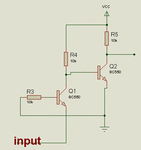
This is a circuit with two transistors that can give a 0 or 5v output controlled by a negative voltage (< -0.7v), maybe you can use it somehow

positive_controlled_by_negative.gif

I have to go to sleep too, talk to you tomorrow.
 

I did some research regarding diode clamping. As it turns out MCHP place restriction to the input impedance to ADC. It varies from 2k5 to 10k depending on the particular MCU. In any case two external Schottky diodes with series resistor of typically 1k should do the trick. Since output of diff OPAMP is limited to 5V by resistor dividers at its input, current from diff OPAMP will be limited to about 5mA in case of reverse polarity which is something easily handled by diff OPAMP and clamping diodes.

I also found interesting discussion at MCHP forum regarding diode clamping in case of high, fast transients which could destabilize power supply. It is easily solved with additional two PNP BJTs. It is not relevant in this case but could be of use to somebody on this forum so I'm adding link to this discussion. https://www.microchip.com/forums/tm.aspx?high=&m=633586&mpage=1#634506

Another good discussion can be found at https://www.ccsinfo.com/forum/viewtopic.php?p=127360

Of course I will have to recalculate correct acquisition time but that's not a problem because math is straightforward.


Now back to the comparator issue...
 
Do you have 2 a/d channels? If you do, you can skip the instrumentation amp and just subtract Bat+ and Bat-
Or, you can use a really neat characteristic of the differential amplifier.
The equation of the differential amp that people usually use is: Vout =(Va-Vb)*(Rf/Ri). However, it is actually Vout =((Va-Vb)*(Rf/Ri))+Vc where Vc is the "ground voltage" of the Rf resistor on the non-inverting input. Normally Vc is ground, but it doesn't have to be. The ground voltage pins are 1 and 5 of the INA117. So if you put pins 1 and 5 at say, 0.25V, then a voltage of "0" on the battery will be 0.25V on the PIC, positive battery voltages will range from 0.25V to 5V and negative battery voltages will be less than 0.25V. Easy to detect in software. OK, now the caveat: the impedance of the resistor divider that sets the 0.25V (or 0.1V, or whatever you choose) must be very low. An opamp is a good choice, or maybe 950 ohm and 50 ohm resistors. TI also shows it in Figure 11 of the INA117 data sheet. Pin 8 still goes to ground.

---------- Post added at 18:41 ---------- Previous post was at 18:12 ----------

A couple more comments. 1) Your boost converter is pretty spooky, I bet. The output range of say 3-50V is a really wide range (duty cycle from 1 down to 0.05). As you know, you have practically no current limit available for low batteries. Have you considered putting an RC on the gate of the MOSFET charger switch and PWM'ing the gate drive when you start so you can use the MOSFET as a poor man's load resistor? It would have to only run for a couple minutes to bring a battery up, and it may save burning off a pc board trace. 2) If you are charging lead acid batteries, your a/d converter doesn't have near enough resolution to support float charge operation (-2mV/deg/cell characteristic, for example). Be careful. 3) Your accuracy is also affected by the resistor dividers feeding the INA117. Since the INA117 can go to a couple hundred volts common mode voltage, why don't you take the (+) input of the INA117 directly to Bat+ and use one divider from Bat- to Bat+ (referenced to Bat+ not to ground). Then there's only a single resistor ratio that sets the value. If you want to maintain a decent untrimmed divider ratio, use identical value surface mount resistors (surface mount resistors on a single strip are nearly identical since they come from one batch), or even better a dip resistor network. Matching on networks is something like 0.1% over temperature (which you won't get even with two different value 0.1% resistors). So to get a 13:1 divider ratio (60V-ish full scale), put 4 10k's in series (40k) and 3 10k's in parallel (3.333k).
 

I really like your idea of offsetting output of OPAMP to provide baseline for software calculation.

I considered adding CMR and offset trimming circuits to INA117 in order to reduce measurement error to a minimum but in the end I decided that it was unnecessary because I really don't need such precision it in this particular circuit. I never thought of using offset to provide baseline for software detection of polarity.

Effective resolution of battery measurement will be lost, of course, but I think it's acceptable. In fact since I intend to use MCU internal FVR set at 4.096V and if offset voltage is 0.1V (or less) it means that I will lose ~2.5 % of effective battery measurement range, which is more than acceptable. And of course one more pin on MCU will be freed for the price of one additional OPAMP and a few precision resistors.

What a simple and elegant solution. Thank you for the great idea.:smile:

As for using two ADC inputs, I considered it initially but I'm not sure that CMRR would match that of the dedicated differential OPAMP like INA117.

---------- Post added at 02:48 ---------- Previous post was at 02:16 ----------

I really like your idea of offsetting output of OPAMP to provide baseline for software calculation.

I considered adding CMR and offset trimming circuits to INA117 in order to reduce measurement error to a minimum but in the end I decided that it was unnecessary because I really don't need such precision it in this particular circuit. I never thought of using offset to provide baseline for software detection of polarity.

Effective resolution of battery measurement will be lost, of course, but I think it's acceptable. In fact since I intend to use MCU internal FVR set at 4.096V and if offset voltage is 0.1V (or less) it means that I will lose ~2.5 % of effective battery measurement range, which is more than acceptable. And of course one more pin on MCU will be freed for the price of one additional OPAMP and a few precision resistors.

What a simple and elegant solution. Thank you for the great idea.:smile:

As for using two ADC inputs, I considered it initially but I'm not sure that CMRR would match that of the dedicated differential OPAMP like INA117.


Regarding you additional comments.

In fact boost converter is PWM controlled by MCU and it's duty cycle is pretty much fixed (although I'm considering implementing some form of MPPT). So, MCU is in fact constantly measuring voltage of the capacitor (resistor divider is not drawn on this simplified schematic) and stops charging process when the capacitor voltage reaches about the twice of the current voltage of the battery. Then it dumps capacitor into the battery. Also, software should take into account voltage on the capacitor, voltage of the battery and calculate energy in Joules discharged to the battery in order to determine how many discharge cycles per second (or rather J/sec) should go to the battery based on the battery data entered by user (voltage, nominal capacity).

I previously tried the process with a simple 555 circuit and as it turns out the battery desulfates quite nicely without excessive heat if there is any chance of reviving it to some extent. Otherwise it starts overheating so of course temperature of the cells is also to be monitored at all times by MCU.

I also considered measuring impedance of the battery in regular time periods to monitor what happens in the cells and if they desulfate properly but to be honest, I haven't found much references in literature of simple method of doing it, so for the moment I'm simply calculating energy discharged into battery and monitor temperature.

I'm aware of the lack of the resolution of the ADC and I considered (I'm still still considering) using higher resolution SPI or I2C ADC. However, for the moment I'm slowly building hardware, then I'm starting on software and if I find it is necessary to use external ADC I did leave one MSSP module free if need arises.

And you're correct about using INA117 common mode to measure voltage directly between the poles of the battery. In fact only today I started considering it after re-reading datasheet but this is just start of the design process and it's likely many more things will change. I like your idea of using resistor networks. I always use precision SMD resistors but I really didn't know that resistor networks have lower temperature drift. Or is it just that all resistors in network are simply drifting by the same value since they are in the same casing?


BTW - poor man's load resistor? You lost me on that one. Could you be so kind to elaborate? I don't think it's relevant in this situation since PWM is pretty much matched to the boost inductor and capacitor but I'm curious of what you were suggesting.
 

1) Resistor drift in dip package - resistors were made at the same time (difference between resistors in package is caused by accuracy of masking process and minute imperfections) and they see the same temperature = identical characteristics.
2) Wow, your boost converter is a *true* charge pump! That's cool. Definitely don't put the RC on the MOSFET since you are switching under load.
3) The poor man's load resistor was because if you have a dead battery and a non-zero boost converter output voltage (boost converter min volts = supply) then you have no current limit so the switching MOSFET would be the limiting impedance. But your dead battery is pretty significant impedance
 

I really like your idea of offsetting output of OPAMP to provide baseline for software calculation.

I have suggested you this solution in post #22
In your first post you mention that in order to measure a negative voltage you use an opamp as inverting amplifier.
An alternative to that is to apply an offset , so suppose that you apply an offset of 0.1v with a differential amplifier, when the input is 0 you will get 0.1 read in the ADC so any reading below 0.1 can be considered a negative voltage , of course you will loose some resolution in the ADC becasue of that offset.

and in post #24 I asked you again about it but you didn't comment on the solution
Any chance to apply the opamp offset?

I suppose you were tired that night and didn't notice it and you didn't review the posts again.

Alex
 
  • Like
Reactions: lighty

    lighty

    Points: 2
    Helpful Answer Positive Rating
Well, somehow I missed it after midnight. :lol:

You're right of course, you did suggest it .;-)
 
Last edited:

Great topic and very interesting reading.
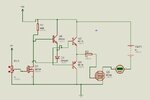
I need to design just a 6V 18Amp battery charger and been looking up on the net and seen so many deisgn's and ideas which some what slightly confusing on the way there done, I want to be able to use mosfet's attached is my drawing. Noy sure if it's the best method, I've not tried yet in real time only in isis(Iknow it's not the best way but just wanted to see if it worked before I built it)
The pot would be replaced with a PWM signal.

Lighty would you be able to give a bit of advise on your set up hardware only for the mosfet drive
batt.JPG

not your source code
wizpic
 

Well, I use PIC MCU's hardware PWM module to drive MOSFET via totem-pole driver consisting of two BJTs (NPN+PNP). There is really nothing special about it. One could use dedicated MOSFET driver IC but I don't see a point in doing that because I'm not switching big power MOSFETs under heavy load. Besides, totem-pole can handle pretty much and by addition of additional resistor and speed-up capacitor it can achieve rather good switching times.
 
Last edited:
  • Like
Reactions: wizpic

    wizpic

    Points: 2
    Helpful Answer Positive Rating
Thanks for that lighty, This was one of my first thoughts to use a totem-pole driver, I shall get something hooked up over the weekend or so and see how things work out. I already have most of the code wrote to take take of the timings and stuff from a previous project that never got completed, So just need to add PWM control and current control for it

wizpic
 

I looked at your schematic once more.

If I understand your idea correctly you want to use MCU PWM to drive IRF640?

IRF640 is a smaller power MOSFET so what you need is just one NPN BJT and two resistors. I have a bunch of 2N2222 in my drawer so I usually use them for driving smaller power MOSFETs (if you're driving larger MOSFET take into account that BJT must be able to handle gate charge currents and choose it accordingly). Then just add appropriate base resistor and collector resistor and connect gate of MOSFET to the collector of BJT. Also add MOSFET series gate resistor in order to reduce possible ringing. What you get is a basic BJT inverting switch and you don't need much more in your case, although you can add speed-up capacitor in parallel to the base resistor if you need to want to make rise and fall edges a bit steeper. There is simply no need for all that circuitry you used in your schematic. One small NPN, two resistors and one optional small capacitor is all you need.

Be aware that it will invert logic of the signal from your MCU output so take that into account in your code. Or you can always add virtualy similar additional stage to the first one (just with a different base resistor value) in order to retain non-inverting logic. I would just take care of that in MCU code if I were you. More parts in your design mean more potential problems, they consume more power, everything is more expensive and it takes more space on PCB. Just remember - KISS ;-)
 
Last edited:

This was just an example of the mosfet driver I would use , I will be using big power fet's for the charger and not the IFR640 may be 3-4 of these fet's just need to hook some up and see how it performs

thanks
wizpic
 

Apart from the discussed gate driver details, which are just O.K. in my view, the circuit in post #35 misses any means for effective PWM operation with a battery load, particularly a storage inductor and a diode.

As shown so far, it's using only the batteries internal resistance to translate duty cycle into average current.
 

Status
Not open for further replies.

Similar threads

Part and Inventory Search

Welcome to EDABoard.com

Sponsor

Back
Top