Continue to Site

Welcome to EDAboard.com

Welcome to our site! EDAboard.com is an international Electronics Discussion Forum focused on EDA software, circuits, schematics, books, theory, papers, asic, pld, 8051, DSP, Network, RF, Analog Design, PCB, Service Manuals... and a whole lot more! To participate you need to register. Registration is free. Click here to register now.

Replace NMOS with PMOS in INVERTER

Status
Not open for further replies.

navink

Newbie level 5
Newbie level 5
Joined
Sep 6, 2012
Messages
9
Helped
0
Reputation
0
Reaction score
0
Trophy points
1,281
Activity points
1,361
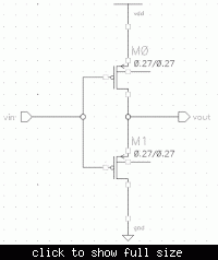
Hi All If we replace the nmos in inverter with pmos what will be the output i.e top pmos source is given to 3.3v supply and its drain is connected to bottom pmos source and bottom pmos drain is ground. Both gates are short and if input =0 what is the output.??
 

Hello navink,

please give a diagramm, what you want to do.

Normally you can not change PMOS to NMOS without changing other parts of the circuit. Also you have an other control signal at the gate.

Regards

Rainer
 

pmos turns off when 1 is applied to the input right so if you are merely going to replace it there are going to be problems as nmos turns on in 1 as ip and off when ip is 0
 

Hello navink,

please give a diagramm, what you want to do.

Normally you can not change PMOS to NMOS without changing other parts of the circuit. Also you have an other control signal at the gate.

Regards

Rainer


33_1346925858.png


Is it possible to connect like this. Vin is 0V

Thanks for your reply

- - - Updated - - -

Hi samuel,

I am asking just what is the output if we connect both pmos in an inverter configuration and apply 0 at the input.
 

if ip is given as 0 then the functionality of the NMOS over PMOS is achieved i agree to that

right now though you have uploaded the image i am not able to view pls will you do it again
 

Both gates are short and if input =0 what is the output.??
You'll want to specify Vth of both transistors first. Assuming enhancement type for both transistors, the output voltage is literally undefined, somewhere between |Vth| and 0.

P.S.: The circuit function is changed from inverter to non-inverting buffer, of course.
 
Last edited:
  • Like
Reactions: navink

    navink

    Points: 2
    Helpful Answer Positive Rating
Hi,

why the output voltage is undefined if the gate of pmos is 0V then it will be ON and it should act like a pass transistor??
 

Since when a MOSFET is on with Vgs of 0 V? It would be only in case of Vth=0.
 

but the top pmos is haviing Vgs of -3.3V then it should be on atleast
 

my boy first check the working of both the NMOS and PMOS completely

PMOS will work alright but what is the threshold voltage of it any way

- - - Updated - - -

my boy first check the working of both the NMOS and PMOS completely

PMOS will work alright but what is the threshold voltage of it any way
 

dont know tell me what happens to threshold voltage
 

I fear the confusion is caused by not posting a schematic.

I thought of changing both transistor polarities, would make sense at least.

A two PMOS transistor circuit is just nonsense, shorting the power supply with 0V input.
 

thanks thats what i am asking is it possible to connect like that if yes then what is the output if no means why no

- - - Updated - - -

thanks thats what i am asking is it possible to connect like that if yes then what is the output if no means why no
 

kindly repost the schematic that will help us all

threshold voltage is the minimum voltage in a NMOS which must be exceeded for the MOS to work it is maximum in the case of PMOS


that is all we can say without looking more in your schematic

- - - Updated - - -

kindly repost the schematic that will help us all

threshold voltage is the minimum voltage in a NMOS which must be exceeded for the MOS to work it is maximum in the case of PMOS


that is all we can say without looking more in your schematic
 

what i am asking is it possible to connect like that
Possible means
- can be done without damaging a transistor?
- serves a reasonable purpose?

As far as I see, we can exclude the second meaning, for the first, depdends on...
 
thanks thats what i am asking is it possible to connect like that
Connect like what? We still can't see your circuit. Please try upload it again.

- - - Updated - - -

Nevermind, I think I cracked it. It was a gimp XCF file saved with a .png extension.

Anyway, here's the circuit the op uploaded:


It looks like a bad idea.
  • If the input is high, then both MOSFETs are off and the output is undefined.
  • If the input is low, then both MOSFETs are on. The top one will be switched on harder, so the output voltage should be pulled high. However a lot of current is wasted and the MOSFETs may burn.
 
Last edited:

Connect like what? We still can't see your circuit. Please try upload it again.

- - - Updated - - -

Nevermind, I think I cracked it. It was a gimp XCF file saved with a .png extension.

Anyway, here's the circuit the op uploaded:


It looks like a bad idea.
  • If the input is high, then both MOSFETs are off and the output is undefined.
  • If the input is low, then both MOSFETs are on. The top one will be switched on harder, so the output voltage should be pulled high. However a lot of current is wasted and the MOSFETs may burn.

Hi godfreyl,

What you said is right both the pmos will be ON but actually one will be in saturation and another in Linear and the transistors wont burn inspite of high current but that high current wil be in the order of uA.

- - - Updated - - -

we can make both the transistors operate in saturation by adjusting their W/L's
 

the operating points of both the MOS then be identical

that is the calibration or the ratings of the MOS must be uniform if variations are there then it would cause some problems

but i must agree that power loss will be high here
 

What you said is right both the pmos will be ON but actually one will be in saturation and another in Linear and the transistors wont burn inspite of high current but that high current wil be in the order of uA.
OK, but it still won't work as an inverter because the output is undefined when the input is high. You would get almost the same results if you left out the bottom MOSFET.
 

Status
Not open for further replies.

Part and Inventory Search

Welcome to EDABoard.com

Sponsor

Back
Top