Continue to Site

Welcome to EDAboard.com

Welcome to our site! EDAboard.com is an international Electronics Discussion Forum focused on EDA software, circuits, schematics, books, theory, papers, asic, pld, 8051, DSP, Network, RF, Analog Design, PCB, Service Manuals... and a whole lot more! To participate you need to register. Registration is free. Click here to register now.

Push Pull Converter with Load - voltage drop Issue

Status
Not open for further replies.
Hi, with 15 watts load the MOSFETs are safe. The signals are clean. The Power supply is ripple free. I have 3*2200uF bypass capacitor along with 1uF Film capacitor. But I see a total disturbance when connecting to 100 watts load. They are not stable at all. I tried adding bypass capacitors directly to the supply terminals, but that didn't help either. This is not only the case with 7AH but also with 150AH. So I think I'm missing something or possibly a layout issue. Here is the image of my design

PCB.jpg COMP.jpg

Sorry for the poor quality.
This is roughly designed one. I'm going through the layout considerations.
This design is just based on everything I could collect. I might be missing something.
 

Hi,

or possibly a layout issue.

I think so. With 100W you have high current pulses with sharp edges.
A gnd_plane is essential. Also short and wide traces in the complete power path: input capacitor, switch, diode, coil, output capacitor and the current path via gnd plane.

Klaus
 
Very Well, I'm Planning for a new Design. I don't have good practice in PCB. I have read few documents though.

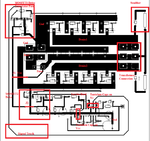
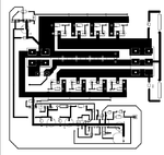
I'll upload my new PCB layout, Could You Please comment on that?

PCB.png PCB2.png

The "signal track" that I have mentioned in Image1 bothers me because the track length have got longer. Is that likely to have any issues with track being so long?
 

Status
Not open for further replies.

Similar threads

Part and Inventory Search

Welcome to EDABoard.com

Sponsor

Back
Top