ErenYeager97
Newbie level 6

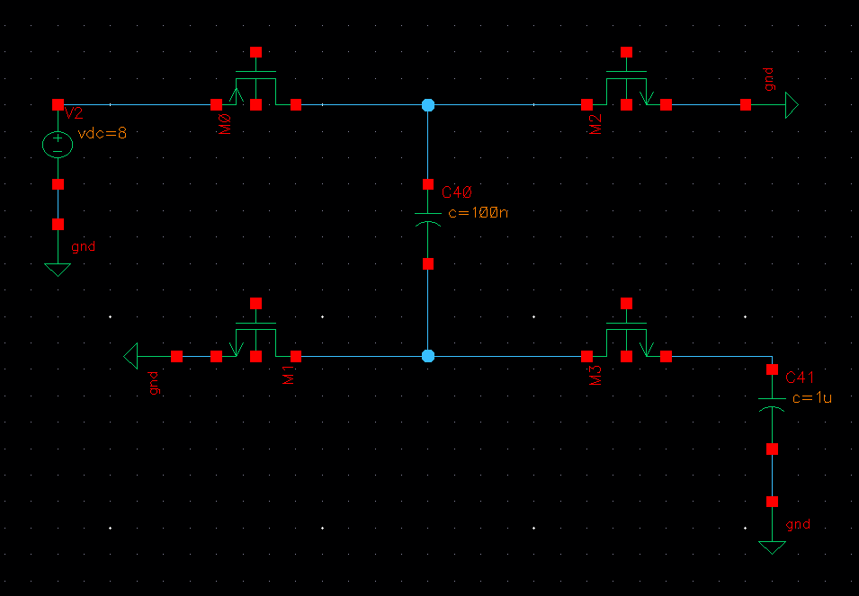
I am trying to design a charge pump inverter (also known as flying capacitor inverter) whi. The idea is simple; using Vdd charge a capacitor in clock phase 1. In clock phase 2, disconnect it from the VDD and simultaneously connect its +ve terminal to ground and -ve terminal to a storage capacitor in clock phase 2. This is shown in the image below:

I have recreated this in Cadence and trying to simulate it.

As can be seen in the left side two switches (upper PMOS and lower NMOS), charge cap to +8V in phase-1. In the phase-2, right side switches (both NMOS), upper one brings +ve terminal to GND, hence at the -ve terminal of the cap, we get develop -8V. This becomes a problem for NMOS switches connected at the lower terminal of the cap.
1st problem: The negative voltage at the cap causes these NMOS to turn on (as the source of NMOS is defined to be the lower potential) if the gate is at 0V
2nd problem: The body/bulk of these NMOS may become forward biased due to the presence of negative voltage at their S/D if not biased to an even lower or equal voltage that is -8V or less (-10V maybe)
Both these issues have been discussed in Texas Instruments LMC7660. I copy the relevant passage from page 6 below:
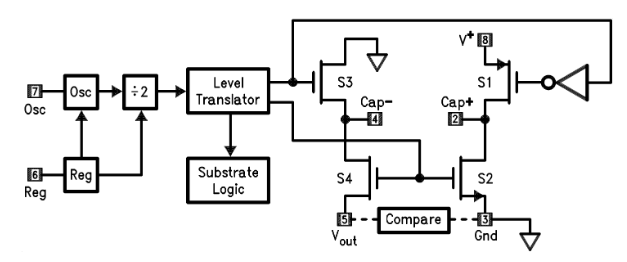
They show in the datasheet how the LMC7660 is designed:

They bias the bulk of S3 and S4 with substrate logic to possibly another -ve voltage and use the level translator to control the gates of these switches.
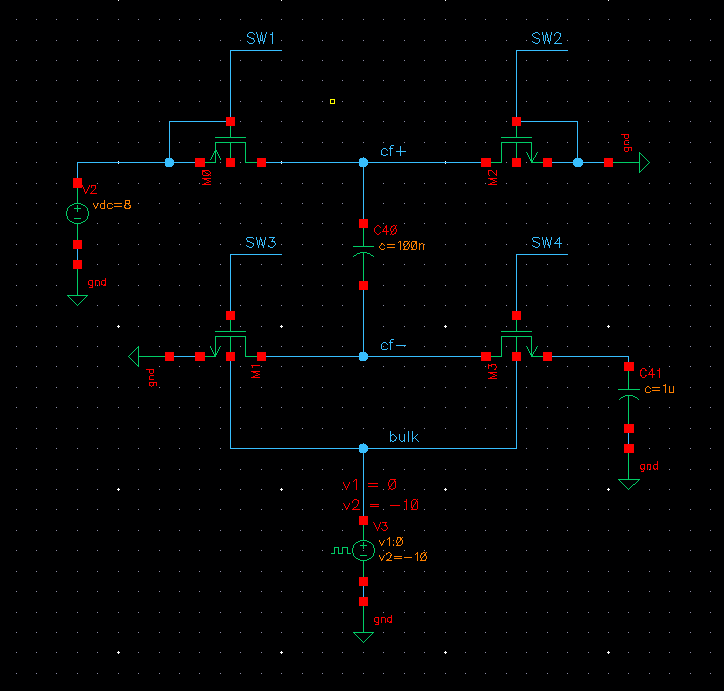
Using this understanding I made another simulation which connects bulk of these switches to a control signal where is phase 1 we bias the lower NMOS switches to 0V and in phase 2 the bulk is tied to -10V. The gate voltages will be generated compared to which terminal has lowest potential.

Right now I am having difficulty with getting it to work. The problem is that the -10V at the bulk appears on the cf- node and on C41 storage capacitor which shouldn't be possible

I have recreated this in Cadence and trying to simulate it.
As can be seen in the left side two switches (upper PMOS and lower NMOS), charge cap to +8V in phase-1. In the phase-2, right side switches (both NMOS), upper one brings +ve terminal to GND, hence at the -ve terminal of the cap, we get develop -8V. This becomes a problem for NMOS switches connected at the lower terminal of the cap.
1st problem: The negative voltage at the cap causes these NMOS to turn on (as the source of NMOS is defined to be the lower potential) if the gate is at 0V
2nd problem: The body/bulk of these NMOS may become forward biased due to the presence of negative voltage at their S/D if not biased to an even lower or equal voltage that is -8V or less (-10V maybe)
Both these issues have been discussed in Texas Instruments LMC7660. I copy the relevant passage from page 6 below:
In the circuit of Figure 11, S1 is a P-channel device and S2, S3, and S4 are N-channel devices. Because the
output is biased below ground, it is important that the p− wells of S3 and S4 never become forward biased with
respect to either their sources or drains. A substrate logic circuit specifies that these p− wells are always held at
the proper voltage. Under all conditions S4 p− well must be at the lowest potential in the circuit. To switch off S4,
a level translator generates VGS4 = 0V, and this is accomplished by biasing the level translator from the S4 p−
well.
They show in the datasheet how the LMC7660 is designed:
They bias the bulk of S3 and S4 with substrate logic to possibly another -ve voltage and use the level translator to control the gates of these switches.
Using this understanding I made another simulation which connects bulk of these switches to a control signal where is phase 1 we bias the lower NMOS switches to 0V and in phase 2 the bulk is tied to -10V. The gate voltages will be generated compared to which terminal has lowest potential.
Right now I am having difficulty with getting it to work. The problem is that the -10V at the bulk appears on the cf- node and on C41 storage capacitor which shouldn't be possible
