Continue to Site

Welcome to EDAboard.com

Welcome to our site! EDAboard.com is an international Electronics Discussion Forum focused on EDA software, circuits, schematics, books, theory, papers, asic, pld, 8051, DSP, Network, RF, Analog Design, PCB, Service Manuals... and a whole lot more! To participate you need to register. Registration is free. Click here to register now.

Overheating LM2596S-5 - Help me fix my first board design

avner_g

Junior Member level 2
Joined
Nov 25, 2023
Messages
22
Helped
0
Reputation
0
Reaction score
0
Trophy points
1
Activity points
227
So I decided I was going to design and build my first PCB and do (yet another) irrigation controller and moisture sensors.
First and foremost, it was great fun. Learning KiCAD, designing everything.

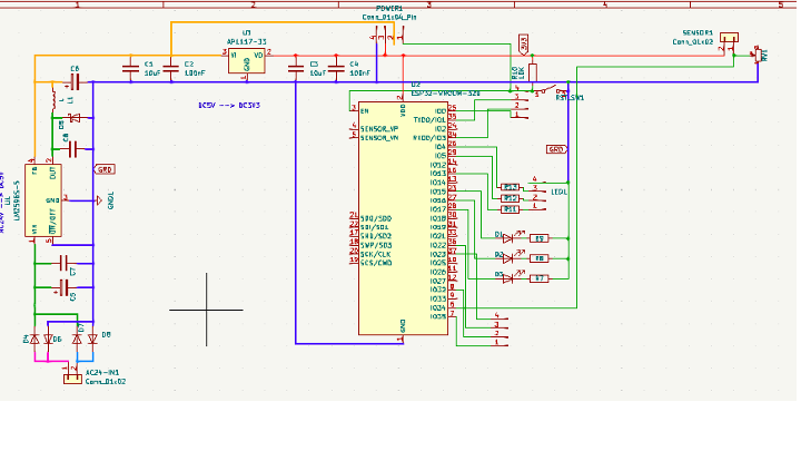
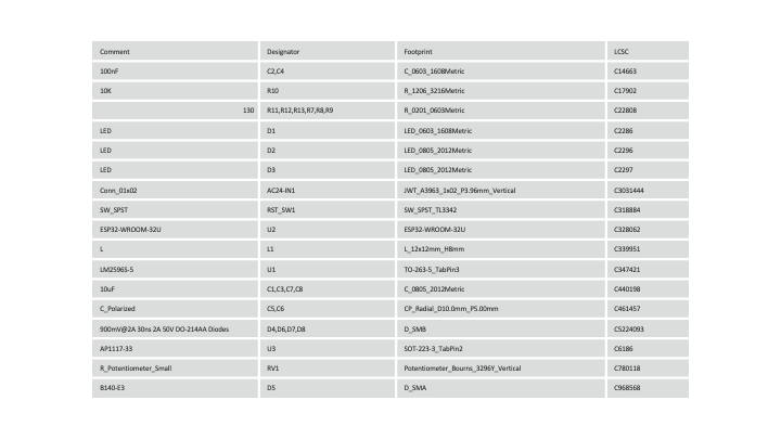
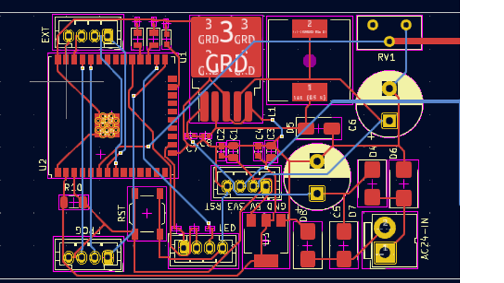
I made the design based on AC24V input (as the pumps require) and, a fairly simple and straightforward diode bridge, and 2 VRegs (to 5V and then 3V3). Here is it: https://github.com/theDontKnowGuy/sprinklers

However, it is not working as expected; the LM2596S-5 (datasheet) got hot in less than a minute to the level I couldn't touch it with my finger. Also a burn smell came out.
I quickly disconnected it and tried another board with AC12V. This time, it got very hot but took longer. Like 2 minutes.

I would appreciate it if you could take a peek at the design https://github.com/theDontKnowGuy/sprinklers to figure out which mistake we made.

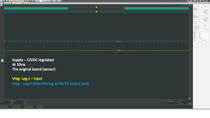
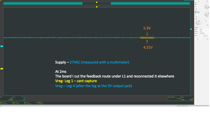
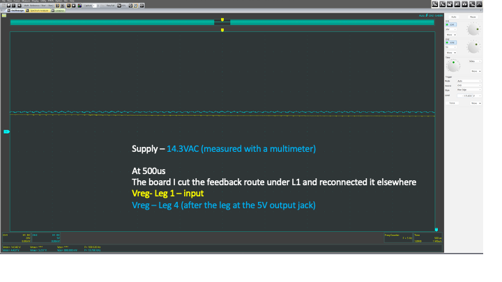
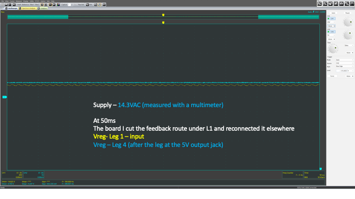
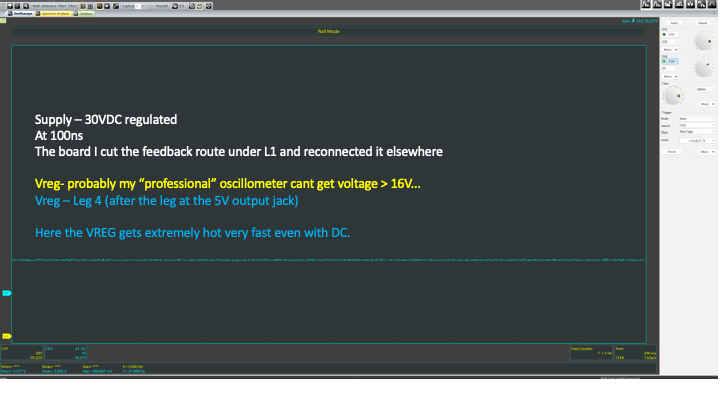
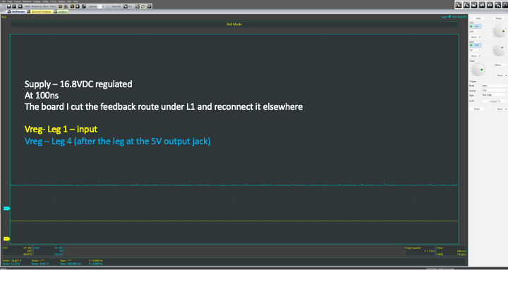
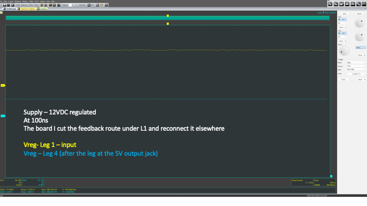
I have made several measurements with my digital oscillometer, which I have also attached.
Someone suggested I run the feedback wire close to the inductor, which I did. I removed it and tried with a strad, but it didn't help either.

The main hint I have is that the over heating occurs also when I supply DC, not only AC.

What I am doing wrong???
Slide1.png
Slide2.png
Slide3.png

Slide1.png
Slide2.png
Slide3.png
Slide4.png
Slide12.png
Slide11.png
Slide10.png
Slide9.png
Slide8.png
Slide7.png
 
So, we are getting there, or at least this is how it feels, thanks to your great guidance.

Here is what I did figure out:

1. @betwixt remark about removing GND lines - done.
2. @KlausST's re-moving GND vias next to the GND pad - done.
3. The only thing I am struggling with about this is @betwixt et al. repeated comment about the heat sinking of the Vreg - I tried following the pattern the footprint of the ESP32 has via holes just below the chip. Do I want to do it differently? If so, how?
4. Trade blue tracks for red ones - done. Now I have minimal blue lines at the top part at the expense of some vias and red routing.
5. @KlausST's re-using C6+ as the +5V hub - done. However not sure about which additional cap I have to add to C6 and where. I already have C8 - 10uF 10V Tantal for the feedback and I read it needs to be close to the VReg FB leg. then have C1 and C2 before the +3V3 VReg. So if need to add an additional one, which spec?

What I didn't figure out:

6. The main point I am now struggling with is @D.A.(Tony)Stewart's concern about the start up on peak voltage. I admit I am not sure what to do with it. I guess the varistor I added at the front is not gonna cover it? If not, would this piece do? https://www.lcsc.com/product-detail/span-style-background-color-ff0-NTC-span-Thermistors_TyoHM-WMF21-33D11MPUP8CB4_C471980.html. instead of the varistor? in addition? where to place?

Thanks again my heroes.
 
Well done for incorporating the suggestions and more importantly, understanding why we made them.

If it's any consolation, even the most professional of us has gone through the same learning stages and I think I can speak for the others in saying we have all made designs that in hindsight we are "less than proud of", I certainly have!

Brian.
 
Hi,

@D.A.(Tony)Stewart:
You say you have concerns about heat.

It´s not clear to me what exactly you mean.
* You calaculate capacitor energy ... and thus loss at power up. So far so good. There are only diodes in sereis, and they usually are rugged enough to handle such capacitive loads.
* then you talk about regulator. There are two. One is the 5V SMPS, the other is the 3.3V linear one.
The switching one - with the new layout - has good heat spreading with the two sides copper area. I expect it to rather relaxed be able to spread 2W. So wit 2W loss we talk about 10W output power. or 2A. I don´t know what´s the drawn output power ... but I expect it to be beow 1A.

* the linear one:1.7V drop x lets say 250mA = about 0.4W. O.K. I guess it becomes hotter than the switcher. (depending on current) Bigger copper area should be easy to implement. and thermal vias.

I did not read the datasheets ... so my thoughts are not confirmed.

Klaus
--- Updated ---

I am thinking only about the hot topic of the simple switcher:

Transient power and steady state power with 24V drop on the switching regulator only, although peak sine can be 32V. There are many unknowns. for resistance but initial load is almost zero as the relays will be off and the LDO won't draw power until the uC starts up with maybe 100 mA. So we have a classical underdamped series RLC network until the relays are commanded on, which might be about 0.5W load each. (1?) There is also a primitive DC moisture sensor and pot with may need C filtering from the inductive noise which I presume is just going into a ADC port.

- transient power on Vin= 24Vac*1.4 @ 90 deg for 5 ms on startup. simple regulator is rated for 3Adc out but output starts at 0V and charges up 470 uF with ~ 50 mohm ESR then aff L1 DCR if = 200 mOhm and diode Rs, transformer DCR all add up to the buck will conduct continuously until the feedback reaches 5V then start switching when after it drops below. But will the stored energy cause it to continue rising with overshoot or will it be underdamped?

Low ESR e-caps have a Tau=ESR*C around 10us in this size but additional parts may extend this to 100 to 200 us. How much current is transferred on startup? What is the charge time? dt=Ic*dV/C There is no soft-start. So if 5V out is charged in 200 us, Ic = CdV/dt = 480 uF*5V/200us = 12Apk. very rough guess...

Will the inductor saturate if operating in DCM mode on startup? Yes
But on steady-state, the duty cycle depends on current and voltage ratio 5V/24 ~20% so operating in DCM mode inductor peaks will be much higher than average.

Ripple spec? I would expect < 50 mVpp but it could be 100 mV.

The datasheet indicates 80 % efficient with 12V and drops with rising input voltages.

Step load tests can be simulated. All PS designs need a power loss budget defined up front. otherwise surprises can occur.
 
Last edited:
Hi,

hmm, I understand. Sounds reasonable.

I never used the LM2596 in my designs.
But:
* I treated them as rather robust devices
* I had to repair some PCBs where they were used ... and defective (exploded). I blamed it on the poor PCB design. But now that you claimed your worries, I´m not sure about this anymore.

Thanks for your explanations.

Klaus
 
So I ordered and received the board and components as prescribed by the good doctors abovementioned.
But I am still running into newbie issues:
After fully soldering the first board, I got a very jumpy voltage at the ESP32. It worked, but not smoothly.
So I decided to build the board step by step and test each step to know what went wrong.
It didn't take long :-/
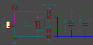
Right after the diode bridge (https://www.lcsc.com/product-detail...de_Vishay-Intertech-ES2A-E3-52T_C5224093.html)
I am confused by the measurements I have made:

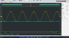
This is the measurement of the input AC voltage without anything connected after the bridge.
Screenshot 2024-01-04 at 11.21.49.png
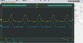
The second I connect the second probe to after the bridge and expect to see "absolute" waves (everything positive), I see this *on both probes*.
Screenshot 2024-01-04 at 11.21.40.png
Clearly, my oscilloscope is crap. But also, I am noticing that one of the diodes is getting hot quickly and, if not disconnected, will smoke up and fry.
Tried it on different copies of the board, with different fresh diodes, getting the same thing. Measured the probes with a multimeter, getting 1M ohms resistance and 0.05nF capacitance on the probes.

What am I missing?
 
Last edited:
Purely a guess without seeing it in the flesh: is one side of your AC input grounded and your scope probe also grounded? If that is the case, you short out one pair of diodes by passing current through the ground wiring.

Brian.
 
You got it right. Now, i after installing the bridge + C5 (470uF 24V) and C7 (25V 1uF MLCC) I am getting a noise at a range of between 500mv and 1V.
Does this make sense in this phase or something is already off?

Screenshot 2024-01-04 at 18.10.10.pngScreenshot 2024-01-04 at 17.48.31.png
 
Noise will come from many sources, including pick-up on the probes themselves, especially when switch mode supplies are nearby. If that is directly across C5/C7 I wouldn't be too concerned because the regulators will drop and clean up the voltages leaving them.

Brian.
 
Post #46 waveform suggest that said 500 mV noise in latest waveform contains a large amount of oscilloscope noise. Don't jump into conclusions.
 

LaTeX Commands Quick-Menu:

Similar threads

Part and Inventory Search

Welcome to EDABoard.com

Sponsor

Back
Top